Introduction to Averatek ASAP Technology
Averatek ASAP (Advanced Semi-Additive Process) is a revolutionary technology that enables the manufacturing of high-density interconnects with trace widths and spaces below 25 microns. This innovative process is transforming the electronics industry by allowing the creation of smaller, faster, and more efficient electronic devices. In this article, we will explore the key features, benefits, and applications of Averatek ASAP technology.
How Averatek ASAP Technology Works
The Semi-Additive Process
Averatek ASAP technology is based on a semi-additive process, which involves the selective deposition of copper on a substrate. The process begins with the application of a thin seed layer of copper on the substrate, followed by the deposition of a photoresist layer. The photoresist is then patterned using photolithography, exposing the areas where the copper traces will be formed.
Next, copper is electroplated onto the exposed areas, forming the desired trace pattern. The photoresist is then removed, and the seed layer is etched away, leaving only the copper traces on the substrate. This process allows for the creation of extremely fine traces with high aspect ratios, enabling the manufacturing of high-density interconnects.
Comparison with Traditional Subtractive Processes
Traditional PCB manufacturing processes, such as subtractive etching, have limitations when it comes to creating fine traces. Subtractive processes involve the removal of unwanted copper from a fully copper-clad substrate, which can lead to undercutting and other issues that limit the minimum achievable trace width.
In contrast, Averatek ASAP technology’s semi-additive process allows for the selective deposition of copper, eliminating the need for etching and enabling the creation of much finer traces. This results in higher-density interconnects and improved signal integrity.

Benefits of Averatek ASAP Technology
Miniaturization and High-Density Interconnects
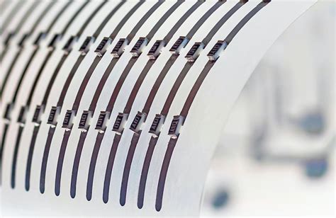
One of the primary benefits of Averatek ASAP technology is its ability to create sub-25 micron traces, enabling the manufacturing of high-density interconnects. This miniaturization allows for the development of smaller, more compact electronic devices, such as smartphones, wearables, and IoT sensors.
Improved Signal Integrity and Reduced Crosstalk
The fine traces and high-density interconnects made possible by Averatek ASAP technology also lead to improved signal integrity and reduced crosstalk. Smaller traces and shorter signal paths result in reduced parasitic capacitance and inductance, which can improve signal quality and reduce signal distortion.
Cost-Effective Manufacturing
Averatek ASAP technology offers a cost-effective solution for manufacturing high-density interconnects. The semi-additive process eliminates the need for expensive materials and equipment associated with traditional subtractive processes, reducing overall manufacturing costs.

Applications of Averatek ASAP Technology
Consumer Electronics
Averatek ASAP technology is particularly well-suited for consumer electronics applications, such as smartphones, tablets, and wearables. The ability to create high-density interconnects enables the development of smaller, more powerful devices with advanced features and functionality.
Automotive Electronics
The automotive industry is increasingly incorporating advanced electronics into vehicles, from infotainment systems to advanced driver assistance systems (ADAS). Averatek ASAP technology can help meet the demand for smaller, more reliable electronic components in this sector.
Medical Devices
Medical devices, such as implantable sensors and wearable health monitors, require small, high-density electronic components. Averatek ASAP technology enables the manufacturing of these components, helping to advance medical technology and improve patient care.
Aerospace and Defense
The aerospace and defense industries require high-performance, reliable electronic components that can withstand harsh environments. Averatek ASAP technology can help meet these demanding requirements by enabling the creation of ruggedized, high-density electronic assemblies.

Case Studies
Case Study 1: Smartphone Manufacturer
A leading smartphone manufacturer implemented Averatek ASAP technology to develop a new, ultra-compact smartphone model. By utilizing sub-25 micron traces, the company was able to significantly reduce the size of the device’s printed circuit board, allowing for a sleeker, more pocket-friendly design. The high-density interconnects also enabled the integration of advanced features, such as 5G connectivity and high-resolution cameras, without compromising the device’s compact form factor.
Case Study 2: Automotive Supplier
An automotive supplier specializing in advanced driver assistance systems (ADAS) adopted Averatek ASAP technology to improve the performance and reliability of their products. The high-density interconnects and improved signal integrity provided by sub-25 micron traces allowed the company to develop more compact, efficient ADAS modules. These modules demonstrated enhanced performance and reduced interference, contributing to safer and more reliable automated driving features.
Future Developments and Trends
As the demand for smaller, more powerful electronic devices continues to grow, Averatek ASAP technology is well-positioned to play a significant role in shaping the future of the electronics industry. Some potential future developments and trends include:
Further Miniaturization
As Averatek ASAP technology continues to evolve, it may enable the creation of even finer traces, potentially reaching sub-10 micron widths. This could lead to even greater miniaturization and higher-density interconnects, enabling the development of even smaller and more advanced electronic devices.
Integration with Other Advanced Manufacturing Technologies
Averatek ASAP technology could be combined with other advanced manufacturing technologies, such as 3D printing and flexible electronics, to create innovative, multi-functional electronic components. This integration could lead to the development of new applications and products that were previously not possible with traditional manufacturing methods.
Expansion into New Industries
While Averatek ASAP technology has already found applications in various industries, such as consumer electronics and automotive, it has the potential to expand into new sectors. For example, the technology could be applied to the development of advanced robotics, smart textiles, and energy storage devices, among others.
Frequently Asked Questions (FAQ)
- What is the minimum trace width achievable with Averatek ASAP technology?
-
Averatek ASAP technology enables the creation of traces with widths below 25 microns, allowing for high-density interconnects and miniaturization of electronic components.
-
How does Averatek ASAP technology differ from traditional subtractive PCB manufacturing processes?
-
Traditional subtractive processes involve the removal of unwanted copper from a fully copper-clad substrate, which can lead to limitations in achieving fine traces. In contrast, Averatek ASAP technology uses a semi-additive process that selectively deposits copper, enabling the creation of much finer traces and higher-density interconnects.
-
What are some of the key benefits of using Averatek ASAP technology?
-
The key benefits of Averatek ASAP technology include miniaturization and high-density interconnects, improved signal integrity and reduced crosstalk, and cost-effective manufacturing.
-
In which industries is Averatek ASAP technology commonly applied?
-
Averatek ASAP technology is commonly applied in industries such as consumer electronics, automotive electronics, medical devices, and aerospace and defense.
-
What are some potential future developments and trends related to Averatek ASAP technology?
- Potential future developments and trends include further miniaturization, integration with other advanced manufacturing technologies, and expansion into new industries.
Conclusion
Averatek ASAP technology represents a significant advancement in the manufacturing of high-density interconnects, enabling the creation of sub-25 micron traces. This innovative technology offers numerous benefits, including miniaturization, improved signal integrity, and cost-effective manufacturing. As the demand for smaller, more powerful electronic devices continues to grow, Averatek ASAP technology is poised to play a crucial role in shaping the future of the electronics industry.
By enabling the development of advanced electronic components across various sectors, from consumer electronics to automotive and medical devices, Averatek ASAP technology is helping to drive innovation and progress. As the technology continues to evolve and expand into new applications, it will undoubtedly contribute to the creation of groundbreaking products and solutions that will transform our world.

Leave a Reply