Introduction to Rigid Flex PCBs
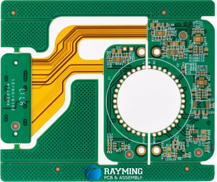
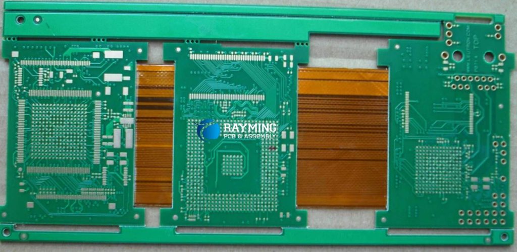
Rigid flex PCBs combine rigid and flexible substrates into a single integrated assembly. It merges circuitry-laden rigid boards with dynamic flexing elements enabled by flexible materials. They deliver connectivity between multiple rigid electronics subassemblies in complex devices where space efficiencies and high interconnectivity are critical needs.
Key Features:
- Rigid areas for component mounting and complex routing
- Flexible areas for dynamic motion or three-dimensional form factors
- Integrated assembly with rigid-flex bends replacing connectors/cables
- High density interconnects where space is limited
Industries using rigid flex PCBs include automotive, aerospace, defense, medical devices, wearables, displays, and IoT devices.
Rigid flex technology allows packing more functionality within the available space. While enabling miniaturization, it also poses new design and manufacturing challenges.
Rigid Flex PCB Materials Overview
Rigid flex PCBs utilize different classes of substrate materials based on the area function:
1. Rigid Substrates: FR-4, high Tg epoxy composites, ceramics or polyimides. They provide mechanical strength for components.
2. Flexible Dielectrics: Polyimide, FEP, PEEK, or PEI based films are commonly used to achieve dynamic flexing capability.
3. Bonding Materials: Adhesives like acrylics, silicones or low flow prepregs integrate the rigid and flex subassemblies.
Compatible thermal expansion properties between material classes is essential for reliability. The needs of conductor lines, bonding layers, cover layers and stiffeners in terms of electrical, mechanical, chemical, and thermal behavior need co-optimization.
Rigid Flex Structures Classification
Rigid flex PCBs can be classified based on flex layer configurations as:
1. Flex-Rigid (Type 1)
A flex circuit (substrate and conductors) with rigid substrates laminated onto one or both sides
2. Rigid-Flex (Type 2)
Two or more rigid boards interconnected using a flex circuit. Dynamic flexible sections connect multiple rigid PCB subassemblies.
3. Rigid-Flex-Rigid (Type 3)
Combines flex-rigid and rigid-flex structuring with flexible circuits extending between top and bottom rigid laminates.
| Structure | Description |
|---|---|
| Flex-Rigid (Type 1) | Flex PCB with Rigid sections on one or both sides |
| Rigid-Flex (Type 2) | Rigid PCBs interconnected through flex layers |
| Rigid-Flex-Rigid (Type 3) | Rigid boards on top/bottom interconnected through middle flex layers |
Rigid Flex Design Essentials
Key considerations in a successful rigid flex PCB design include:
1. Define Flex Requirements
Determining the flexing zones, dimensions, dynamic motion cycles, and required lifetime durability. Environmental conditions need factoring too.
2. Stackup Development
Choice of material properties and dimensions including flex dielectric films, bonding films, cover layers and stiffeners based on electrical, thermal and mechanical needs.
3. Understand Fabrication Process Capabilities
Knowledge of manufacturer design rules for line width/space, metal foil types, panel utilization, panel and hole sizes restrictions.
4. Manage Transitions
Proper management of transitions between rigid and flex areas in terms of reducing mechanical stress concentration and preventing electrical reflections.
5. Account for Circuit Performance Stresses
Performance analysis modeling various use state conditions – static and dynamic bending, twist/torsion effects, vibration exposure, drop shock, etc.
With increasing complexity, predictive modeling via simulation helps make informed design decisions.
Top 10 Rigid Flex Design Guidelines
Here are key PCB design guidelines for reliable complex rigid flex boards:
1. Define Rigid vs Flex Areas Upfront: Clearly identify rigid and flexible zones including component placements early. Allows optimizing stackup materials accordingly.
2. Design Rigid Layers First: Complete signal routing, plane definition, layer stack and DFM checks on rigid layers before integrating flex layers.
3. Minimize Asymmetric Stacking: Balance metal/dielectric layers above and below core layer throughout rigid and flex sections to mitigate warpage from asymmetric construction.
4. Watch Trace Dimensions at Transitions: Use tear-drop patterns in flex layers with smooth graduation for traces entering/exiting rigid sections. Avoid sharp corners.
5. Include Stabilization Features: Incorporate cross-hatched copper fills, non-functional traces, metal/dielectric compensation shapes to ease rigid-flex transitions.
6. Define Flex Bend Areas: Specify precise flexible hinge locations, arrange circuits to clear openings. Avoid components at bends. Leave ~0.2mm web between openings.
7. Analyze Flex Dynamic Motions: Use minimum bend radius data from manufacturer to model various use conditions – folding, twisting, vibration, shock/drop events near rigid-flex junctions.
8. Review Adhesive Selections: Ensure rigid-flex bonding adhesives can withstand temperature extremes, prolonged vibration, mechanical shocks and humidity expected during product lifecycle.
9. Leave Margins around Rigid Edges: Provide sufficient extra margins ~0.5-1mm around rigid board profiles to account for dimensional variability during processing.
10. Perform DFM Analysis for Manufacturability: Rigid flex designs require extensive DFM analysis together with board shops to avoid design-manufacturing gaps before release.
Rigid Flex PCB Layout Considerations
Here are some key layout considerations when designing complex rigid flex boards:
1. Board Outline and Profiles
Define overall rigid-flex envelope (Length x Width) respecting equipment process limits. If panels, allow street widths for separation routers. Define rigid layer profiles accounting for fabrication process tolerances (~0.3mm). Use tabs/bridges to temporarily hold rigid-flex layers together before routing complex shapes (rectangles easier).
2. Trace Routing Under Flex Area
Unless specified, avoid having traces routed in rigid layers under dynamic flexing areas. Copper flexing repeatedly risks fatigue related opens.
3. annular Ring Control
Ensure complete well-defined annular rings/copper wraps around drilled holes especially at rigid-flex transitions where registration becomes challenging.
4. Solder Mask Pullback
Use solder mask pullback (tenting) around pad perimeters to prevent mask cracking at rigid/flex junctions. Typical pullback is 0.1 mm.
5. Copper Balancing
Maintain copper balance across board including both rigid and flex areas to prevent warpage from asymmetric construction. Miss-registration risks grow with excessive warpage.
6. Breakout Structures
For high layer count rigid-flex designs, implement breakout tab type pad structures on surface layers over 25μm thin core dielectrics to mitigate drilling challenges and capture pad reliability concerns.
7. Stiffener Integration
Incorporate metallic stiffeners/carrier frames around perimeter rigid sections for mechanical strength. Needs isolation from active circuits.
Fabrication Process Steps Overview
Rigid flex PCB manufacturing bridges rigid PCB fabrication technology with flex circuit processing combining the following common steps:
1. Material Preparation
Cutting dielectric layers like polyimide to required shapes (rectangles/complex profiles). Conductor materials also readied respectively.
2. Surface Treatment
Processes like chemical or plasma etching prepare material surfaces improving adhesion.
3. Imaging and Etching
Lithography techniques like photoimaging, laser direct imaging or inkjet printing transfer conductor patterns onto cores followed by etching process to isolate circuits.
4. Hole Drilling
Mechanical or laser processing creates drilled holes for electrical interconnections across structure. Precise depth control to avoid hitting subsequent layers.
**5. Plating Metallization using electroless copper with electrolytic copper builds interconnect walls through drilled holes and increase conductor thickness to required levels.
6. Lamination
Bonding of cores, prepregs using precise temperature, pressure and position control to integrate flex-rigid materials into finished form.
7. Patterning and Etching
Additional imaging and etching steps build up outer layer circuitry on panel. Inner layer connections completed earlier.
8. Solder Mask and Legend Printing
Ultraviolet light selective coating of solder mask, legend printing and carbon ink conductive edge definition.
9. Final Metal Finishes
Surface finishes like ENIG, immersion tin or gold enhance solder joint reliability and protect copper traces from corrosion risks.
10. Electricsl Testing
Validates quality – opens, shorts testing and confirming layer-to-layer connections.
11. Final Shaping/Routing
Precision routing isolates boards from panel transforming profiles from rectangular to required contours including any board cutouts. Additional flash cleaning process removes residues.
12. Final Testing and Inspection QC validation confirming electrical performance along with visual and magnification inspection assessing fabrication quality against IPC standards.
Key Rigid Flex PCB Design Software Tools
Modern PCB design tools integrating MCAD, signal/power integrity analysis and DFM checks are essential for complex rigid flex development. They enhance design efficiency, reduce error risks and allow predictive modeling of product behavior under use conditions.
Popular rigid flex design software options include:
1. Altium Designer
Unified electronics design platform with native 3D modeling, multiboard connectivity spanning rigid-flex boards. Automates manufacturing documentation.
2. Cadence Allegro PCB Designer
Scalable solution tailored for multilayer rigid flex boards including analysis, DFM checks and manufacturing collaboration niceties.
3. Mentor Xpedition
Integrates schematic capture, layout, wiring harness data with MCAD collaboration features ideal for multifunction rigid flex products.
4. Siemens NX Electronics Design
Combines electrical and mechanical domain design tools for concurrent development of rigid flex structures.
Tool evaluation versions allow testing specific capabilities before purchase decisions suiting product design needs. Cloud-hosted tools also gaining traction.
FQA
Q1. What are some examples of rigid flex PCB applications?
A1. Some common applications are:
- Foldable displays in consumer devices
- Printed circuit board cameras
- Automotive camera modules
- Defense electronics in missiles
- Medical ultrasound array probes
- Industrial robot arms
Rigid flex PCBs support dynamic motion needs coupled with dense routing capabilities in space constrained environments across industries.
Q2. What are some limitations of using FR-4 materials in flex PCB sections?
A2. Some FR-4 material limitations for dynamic flexing include:
- Higher modulus risks fracture during bending
- Low glass transition temperature causing cracks
- Moisture absorption decreasing insulation resistance
- Higher weight compared to polyimides
FR-4 glass-epoxy, being economical, can support simpler infrequent flex requirements. Polyimides suit more critical applications.
Q3. What are common cover layer options used over flex layers in rigid flex boards?
A3. Typical rigid flex cover layer (solder mask replacement) materials include:
- Liquid photo imagable solder masks (LPSM)
- Dry film solder mask
- Coverlay composites like acrylics and polyimides
Cover layers protect delicate flex conductor traces from handling, deposits and environmental damage. Some allow soldering also.
Q4. What special analyses are crucial for reliable rigid flex designs?
A4. Vital analyses to validate complex rigid flex designs include:
- Board stress/strain analysis
- Vibration fatigue assessment
- Thermal cycling simulations
- Shock & drop impact analysis
- Signal integrity analysis
- Manufacturing process modeling
Such modeling under use environmental conditions allows predictive assessment of reliability risks early in the design phase.
Q5. What are some common defects occurring in rigid flex boards?
A5. Typical rigid flex process defects include:
- Layer misregistration at rigid-flex transitions
- Insufficient adhesive fill between layers
- Drilled hole quality issues like wall pull away
- Conductor fractures under flexing zones
- Cracks in brittle solder mask or bonding films
- Contamination reducing insulation resistance
Controlling process variability and material compatibility helps mitigate such defects.
Leave a Reply