
Introduction to Rigid-Flex PCB Design
Rigid-flex PCBs are a combination of rigid and flexible printed circuit boards that offer unique advantages over traditional rigid PCBs. These boards consist of rigid sections connected by flexible sections, allowing for enhanced reliability, improved signal integrity, and reduced overall package size. Rigid-flex PCBs find applications in various industries, including aerospace, automotive, medical devices, and consumer electronics.
In this article, we will explore the key aspects of rigid-flex PCB design, focusing on command set-up and layer stack design. By understanding these critical elements, designers can effectively create reliable and efficient rigid-flex PCBs that meet the specific requirements of their applications.
Advantages of Rigid-Flex PCBs
Reduced Size and Weight
One of the primary advantages of rigid-flex PCBs is their ability to reduce the overall size and weight of electronic assemblies. By combining rigid and flexible sections, designers can create more compact packages that occupy less space and weigh less than traditional rigid PCBs. This is particularly beneficial in applications where size and weight are critical factors, such as in aerospace and portable devices.
Enhanced Reliability
Rigid-flex PCBs offer enhanced reliability compared to traditional rigid PCBs. The flexible sections of the board allow for greater flexibility and stress relief, reducing the risk of component failures due to mechanical stress or vibration. Additionally, the elimination of connectors between rigid sections improves signal integrity and reduces the potential for connection-related issues.
Improved Signal Integrity
The use of rigid-flex PCBs can significantly improve signal integrity in electronic systems. By eliminating connectors and reducing the overall length of signal paths, designers can minimize signal reflections, crosstalk, and electromagnetic interference (EMI). This is especially important in high-speed applications where signal integrity is crucial for proper system operation.
Cost Reduction
Although the initial design and fabrication costs of rigid-flex PCBs may be higher than traditional rigid PCBs, they can lead to overall cost savings in the long run. The reduced size and weight of rigid-flex PCBs can result in lower shipping and handling costs. Additionally, the improved reliability and reduced need for connectors can lead to lower maintenance and repair costs over the product’s lifetime.
Rigid-Flex Command Set-up
Design Software and Tools
To design rigid-flex PCBs effectively, designers need to use specialized design software and tools that support rigid-flex capabilities. Some popular PCB design software packages that offer rigid-flex support include:
- Altium Designer
- Cadence Allegro
- Mentor Graphics PADS
- Zuken CR-8000
These software tools provide specific features and capabilities that streamline the rigid-flex design process, such as 3D modeling, layer stack management, and design rule checks (DRCs) specific to rigid-flex designs.
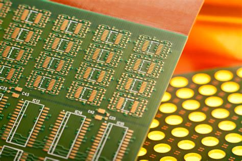
Layer Stack Configuration
The layer stack configuration is a critical aspect of rigid-flex PCB design. It determines the number and arrangement of conductive layers, dielectric materials, and adhesives used in the construction of the board. A typical rigid-flex layer stack consists of the following elements:
- Rigid layers: These are the standard FR-4 or other rigid PCB materials used in the rigid sections of the board.
- Flexible layers: These are the flexible substrates, such as polyimide or polyester, used in the flexible sections of the board.
- Adhesive layers: These are the bonding materials used to laminate the rigid and flexible layers together.
- Coverlay: This is an insulating material applied to the outer surfaces of the flexible sections to protect the circuitry.
Designers must carefully consider the layer stack configuration to ensure proper functionality, reliability, and manufacturability of the rigid-flex PCB.
Material Selection
Selecting the appropriate materials for rigid-flex PCBs is essential for achieving the desired performance and reliability. The choice of materials depends on various factors, including the application requirements, operating environment, and budget constraints. Some common materials used in rigid-flex PCBs include:
- FR-4: A popular rigid PCB material known for its good mechanical and electrical properties.
- Polyimide: A flexible substrate material with excellent thermal stability and chemical resistance.
- Polyester: Another flexible substrate material that offers good flexibility and durability.
- Adhesives: Various adhesive materials, such as acrylic and epoxy, are used to bond the rigid and flexible layers together.
Designers should work closely with their PCB fabricators to select the most suitable materials for their specific rigid-flex designs.
Design Rules and Constraints
Rigid-flex PCB design requires adherence to specific design rules and constraints to ensure proper manufacturability and reliability. Some key design rules and constraints to consider include:
- Minimum trace width and spacing: These rules ensure that the traces on the PCB are sufficiently wide and spaced apart to prevent short circuits and signal integrity issues.
- Minimum bend radius: This rule specifies the smallest allowable radius for the flexible sections of the board to prevent excessive stress and damage during flexing.
- Copper balance: Maintaining a balanced copper distribution across the layers helps prevent warpage and other manufacturing defects.
- Teardrops and anchoring: Adding teardrops at trace-to-pad junctions and anchoring traces to pads improves the mechanical strength and reliability of the connections.
Designers should familiarize themselves with the specific design rules and constraints provided by their PCB fabricators to ensure compliance and optimal results.

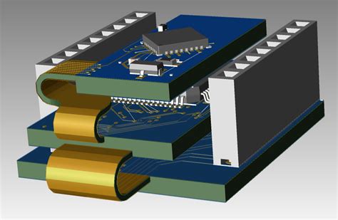
Layer Stack Design
Rigid and Flexible Layer Arrangement
The arrangement of rigid and flexible layers in a rigid-flex PCB is a critical factor in determining the board’s functionality and reliability. Designers must consider the placement of components, routing of signals, and mechanical requirements when deciding on the layer arrangement.
A common approach is to place the rigid layers on the outer surfaces of the board, with the flexible layers sandwiched between them. This arrangement provides structural support for the components and allows for the flexible sections to be routed between the rigid sections.
Signal Integrity Considerations
Signal integrity is a crucial consideration in rigid-flex PCB design, particularly in high-speed applications. Designers must carefully plan the routing of signals to minimize signal reflections, crosstalk, and EMI.
Some strategies for improving signal integrity in rigid-flex PCBs include:
- Minimizing the length of signal paths, particularly in the flexible sections.
- Using controlled impedance traces to match the impedance of the source and load.
- Employing differential signaling techniques to reduce noise and improve noise immunity.
- Implementing proper grounding and shielding techniques to minimize EMI.
Designers should also consider the impact of the flexible sections on signal integrity, as the bending and flexing of the board can affect the electrical properties of the traces.
Thermal Management
Thermal management is another important consideration in rigid-flex PCB design. The flexible sections of the board can act as thermal barriers, limiting the heat dissipation from components in the rigid sections.
To address thermal management challenges, designers can:
- Use thermal vias to provide a heat transfer path from the components to the outer layers of the board.
- Incorporate heat spreaders or heat sinks in the rigid sections to improve heat dissipation.
- Select materials with appropriate thermal conductivity properties for the specific application.
Proper thermal management helps ensure the long-term reliability and performance of the rigid-flex PCB.
Manufacturability and Cost Optimization
Designing rigid-flex PCBs with manufacturability and cost optimization in mind is essential for successful production and deployment. Designers should consider the following factors to improve manufacturability and reduce costs:
- Minimizing the number of layers in the stack-up to reduce complexity and fabrication costs.
- Using standard materials and processes whenever possible to leverage existing manufacturing capabilities.
- Avoiding tight tolerances and small feature sizes that may increase fabrication costs and lead times.
- Optimizing panel utilization to maximize the number of boards per panel and reduce material waste.
Collaborating closely with PCB fabricators and assembly partners can help designers identify opportunities for manufacturability and cost optimization throughout the design process.
FAQ
Q1: What are the benefits of using rigid-flex PCBs over traditional rigid PCBs?
A1: Rigid-flex PCBs offer several benefits, including reduced size and weight, enhanced reliability, improved signal integrity, and potential cost savings in the long run.
Q2: What software tools are commonly used for rigid-flex PCB design?
A2: Popular PCB design software packages that support rigid-flex capabilities include Altium Designer, Cadence Allegro, Mentor Graphics PADS, and Zuken CR-8000.
Q3: What materials are typically used in rigid-flex PCBs?
A3: Common materials used in rigid-flex PCBs include FR-4 for rigid sections, polyimide and polyester for flexible sections, and various adhesives for bonding the layers together.
Q4: What are some key design rules and constraints to consider in rigid-flex PCB design?
A4: Key design rules and constraints include minimum trace width and spacing, minimum bend radius, copper balance, and the use of teardrops and anchoring to improve mechanical strength and reliability.
Q5: How can designers address thermal management challenges in rigid-flex PCBs?
A5: Designers can address thermal management challenges by using thermal vias, incorporating heat spreaders or heat sinks, and selecting materials with appropriate thermal conductivity properties.
Conclusion
Rigid-flex PCB design offers numerous advantages over traditional rigid PCBs, including reduced size and weight, enhanced reliability, improved signal integrity, and potential cost savings. To successfully design rigid-flex PCBs, designers must understand the key aspects of command set-up and layer stack design.
By using specialized design software and tools, selecting appropriate materials, and adhering to specific design rules and constraints, designers can create reliable and efficient rigid-flex PCBs that meet the unique requirements of their applications. Careful consideration of layer arrangement, signal integrity, thermal management, and manufacturability is essential for optimal results.
As the demand for compact, reliable, and high-performance electronic systems continues to grow, rigid-flex PCB design will play an increasingly important role in enabling the next generation of innovative products and technologies.
Leave a Reply