What is a PCB Trace?
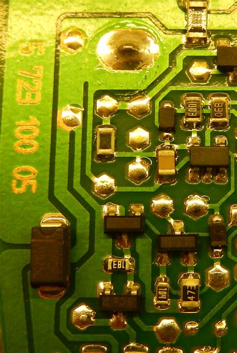
A PCB trace, also known as a copper trace or circuit trace, is a thin strip of copper that carries electrical signals between components on a printed circuit board (PCB). These traces are essential for the proper functioning of electronic devices, as they provide the necessary connections between various components such as resistors, capacitors, integrated circuits (ICs), and connectors.
PCB traces are typically made from copper due to its excellent electrical conductivity and relatively low cost. The thickness and width of these traces depend on factors such as the current-carrying requirements, signal integrity, and PCB manufacturing constraints.
Types of PCB Traces
There are several types of PCB traces, each serving a specific purpose in the overall design of a circuit board. Some common types include:
-
Signal Traces
Signal traces are used to carry low-power, high-frequency signals between components on a PCB. These traces are usually narrow and have controlled impedance to maintain signal integrity.
-
Power Traces
Power traces are designed to carry higher currents and distribute power to various components on the PCB. These traces are typically wider than signal traces to accommodate the increased current flow and minimize voltage drop.
-
Ground Traces
Ground traces provide a common reference point for electrical signals and help to minimize electromagnetic interference (EMI) and crosstalk between adjacent traces. These traces are often connected to a ground plane layer in the PCB.
PCB Trace Design Considerations
When designing PCB traces, several factors must be taken into account to ensure proper functionality, reliability, and manufacturability of the circuit board.
Trace Width and Thickness
The width and thickness of PCB traces are crucial parameters that affect their current-carrying capacity, resistance, and impedance. Wider traces can carry more current and have lower resistance, while thinner traces are better suited for high-frequency signals and dense PCB layouts.
The thickness of a PCB trace is determined by the copper weight, which is typically measured in ounces per square foot (oz/ft²). Common copper weights for PCBs range from 0.5 oz/ft² to 2 oz/ft², with 1 oz/ft² being the most widely used.
To calculate the appropriate trace width for a given current requirement, designers can use a trace width calculator or refer to industry standards such as IPC-2221.
Trace Spacing and Clearance
Proper spacing between PCB traces is essential to prevent short circuits, minimize crosstalk, and ensure manufacturability. The minimum trace spacing depends on factors such as the PCB fabrication process, voltage requirements, and environmental conditions.
Clearance refers to the minimum distance between a trace and other conductive features on the PCB, such as pads, vias, and planes. Adequate clearance helps to prevent unintended connections and reduces the risk of electrical shorts.
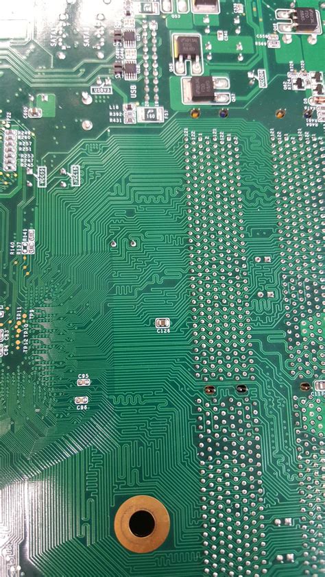
Trace Routing
PCB trace routing is the process of creating interconnections between components on a circuit board while adhering to design rules and constraints. Proper trace routing is critical for maintaining signal integrity, minimizing EMI, and ensuring reliable operation of the electronic device.
Some key considerations for trace routing include:
- Minimizing trace length to reduce signal delay and attenuation
- Avoiding sharp corners and using smooth bends to minimize reflections and impedance discontinuities
- Using via-in-pad or blind/buried vias to optimize space utilization and reduce trace length
- Implementing differential pair routing for high-speed signals to maintain signal integrity
PCB Trace Manufacturing Process
The manufacturing process for PCB traces involves several steps, each of which contributes to the overall quality and reliability of the final product.
Copper Foil Lamination
The first step in creating PCB traces is to laminate a thin layer of copper foil onto the surface of the PCB substrate material, which is typically made of FR-4 or other glass-reinforced epoxy laminates. The copper foil is bonded to the substrate using heat and pressure, forming a strong and uniform adhesion.
Photolithography
After the copper foil is laminated, a photoresist layer is applied to the surface of the copper. The photoresist is then exposed to UV light through a photomask, which contains the desired trace pattern. The exposed areas of the photoresist become soluble and can be removed using a developer solution, leaving the unexposed areas intact.
Etching
Once the photoresist pattern is developed, the PCB is subjected to an etching process, which removes the unwanted copper from the surface of the board. The most common etching method is chemical etching, which uses a solution of ferric chloride or ammonium persulfate to dissolve the exposed copper.
Photoresist Removal and Cleaning
After etching, the remaining photoresist is stripped from the surface of the PCB using a chemical stripper or mechanical abrasion. The board is then cleaned to remove any residual contaminants and prepared for the next steps in the manufacturing process, such as Solder mask application, silkscreen printing, and surface finish.

PCB Trace Testing and Inspection
To ensure the quality and reliability of PCB traces, various testing and inspection methods are employed during and after the manufacturing process.
Continuity Testing
Continuity testing is performed to verify that all the required electrical connections between components are present and functioning correctly. This test is typically done using a multimeter or a dedicated continuity tester, which checks for a low-resistance path between two points on the PCB.
Isolation Testing
Isolation testing is conducted to ensure that there are no unintended short circuits or leakage paths between adjacent traces or components. This test is usually performed using a high-voltage insulation resistance tester, which applies a specified voltage between two points and measures the resistance to detect any insulation breakdowns or leakage currents.
Automated Optical Inspection (AOI)
AOI is a non-contact inspection method that uses high-resolution cameras and advanced image processing algorithms to detect defects and anomalies on the surface of the PCB. AOI systems can identify issues such as missing or misaligned components, solder bridges, and trace defects, allowing for early detection and correction of manufacturing problems.
X-ray Inspection
X-ray inspection is used to examine the internal structure of a PCB, particularly for multi-layer boards with hidden traces and vias. This non-destructive testing method can detect issues such as voids in solder joints, broken traces, and misaligned or missing components that may not be visible from the surface of the board.
Frequently Asked Questions (FAQ)
-
What is the difference between a PCB trace and a wire?
A PCB trace is a flat, thin strip of copper that is etched onto the surface of a printed circuit board, while a wire is a standalone conductor that is typically insulated and used to connect components or PCBs. PCB traces are an integral part of the circuit board, whereas wires are separate components that are added to the board during assembly. -
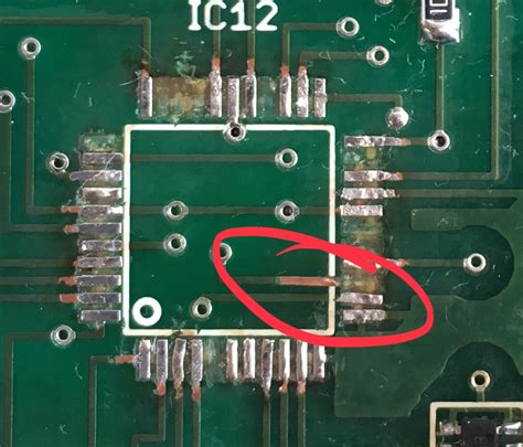
Can PCB traces be repaired if damaged?
In some cases, damaged PCB traces can be repaired using techniques such as jumper wires, conductive epoxy, or micro-soldering. However, the feasibility and effectiveness of the repair depend on factors such as the extent of the damage, the location of the trace, and the accessibility of the affected area. In many cases, it may be more cost-effective to replace the damaged PCB entirely. -
What is the difference between a single-sided and double-sided PCB in terms of traces?
A single-sided PCB has traces on only one side of the board, while a double-sided PCB has traces on both sides. Double-sided PCBs offer more routing options and higher component density compared to single-sided boards, as traces can be placed on both the top and bottom layers. However, double-sided PCBs are more complex to design and manufacture, and they may require additional vias to connect traces on opposite sides of the board. -
How do you calculate the resistance of a PCB trace?
The resistance of a PCB trace can be calculated using the following formula:
R = ρ * L / (W * T)
Where:
– R is the resistance of the trace in ohms (Ω)
– ρ is the resistivity of the copper material (1.68 x 10^-8 Ω•m for pure copper)
– L is the length of the trace in meters (m)
– W is the width of the trace in meters (m)
– T is the thickness of the trace in meters (m)
- What is the purpose of a ground plane in a PCB, and how does it affect traces?
A ground plane is a large area of copper on a PCB layer that is connected to the ground potential of the circuit. The purpose of a ground plane is to provide a low-impedance return path for electrical currents, minimize electromagnetic interference (EMI), and improve signal integrity. Ground planes also help to reduce the loop area of traces, which can minimize the inductance and radiation of high-frequency signals. When designing traces on a PCB with a ground plane, it is important to consider factors such as trace-to-plane spacing, trace impedance, and the placement of vias to ensure optimal performance.
Leave a Reply