Introduction to PCB Manufacturing
Printed Circuit Boards (PCBs) are the backbone of modern electronics. They provide a platform for electrical components to be mounted and interconnected to form a functional circuit. The PCB manufacturing process involves several steps, from design and fabrication to assembly and testing. In this article, we will explore the various processes involved in PCB manufacturing, with a special focus on the wave soldering technique.
PCB Fabrication Process
The PCB fabrication process begins with the design of the circuit board. The design is created using specialized software, such as Eagle or KiCad, which generates the necessary files for manufacturing. These files include the Gerber files, which contain information about the copper layers, drill holes, and silkscreen, and the drill files, which specify the location and size of the holes to be drilled in the board.
Once the design is finalized, the fabrication process can begin. The first step is to create a copper-clad laminate, which is a sheet of insulating material, typically fiberglass, coated with a thin layer of copper on one or both sides. The copper layer is then etched away in a pattern that corresponds to the desired circuit layout, leaving only the necessary copper traces.
Etching Methods
There are two main methods for etching the copper layer: subtractive and additive.
In the subtractive method, the entire copper layer is coated with a photoresist material, which is then exposed to UV light through a photomask that contains the circuit pattern. The exposed areas of the photoresist are then removed, leaving the copper layer exposed in the desired pattern. The board is then placed in an etching solution, which removes the exposed copper, leaving only the desired traces.
In the additive method, the copper layer is first completely removed from the laminate. A photoresist is then applied and exposed through a photomask, just like in the subtractive method. However, instead of etching away the exposed copper, the board is placed in an electroplating bath, which deposits copper onto the exposed areas, building up the desired traces.
| Method | Advantages | Disadvantages |
|---|---|---|
| Subtractive | – Faster and cheaper than additive method – Can produce finer traces |
– Waste of copper – Environmentally unfriendly |
| Additive | – Minimal waste – Environmentally friendly |
– Slower and more expensive than subtractive method – Cannot produce traces as fine as subtractive method |
Drilling and Plating
After the copper layer has been etched, the next step is to drill holes in the board for through-hole components and vias. The drilling is done using a specialized machine that can drill multiple holes simultaneously with high precision.
Once the holes have been drilled, they need to be plated with a conductive material, typically copper, to provide electrical continuity between the layers of the board. This is done through a process called electroless plating, where the board is immersed in a chemical bath that deposits a thin layer of copper onto the walls of the drilled holes.
Solder Mask and Silkscreen
The final steps in the PCB fabrication process are the application of the solder mask and silkscreen. The solder mask is a protective layer that covers the copper traces, leaving only the areas where components will be soldered exposed. This helps to prevent short circuits and makes the soldering process easier.
The silkscreen is a layer of text and symbols that is printed onto the surface of the board to aid in assembly and troubleshooting. It typically includes component labels, polarity markers, and other useful information.
PCB Assembly Process
Once the PCB fabrication process is complete, the board is ready for assembly. The assembly process involves soldering components onto the board and testing the completed circuit for functionality.
Component Placement
The first step in the assembly process is to place the components onto the board. This can be done manually for small runs or prototypes, but for larger production runs, automated machines are used. These machines use computer vision and precision robotics to place the components onto the board with high accuracy and speed.
Soldering Methods
Once the components have been placed, they need to be soldered onto the board to create electrical connections. There are several methods for soldering components onto a PCB, each with its own advantages and disadvantages.
| Method | Advantages | Disadvantages |
|---|---|---|
| Hand Soldering | – Flexible and customizable – Suitable for small runs and repairs |
– Slow and labor-intensive – Inconsistent quality |
| Reflow Soldering | – Fast and automated – Suitable for surface mount components |
– Requires specialized equipment – Not suitable for through-hole components |
| Wave Soldering | – Fast and automated – Suitable for through-hole components |
– Can damage sensitive components – Requires careful design and preparation |

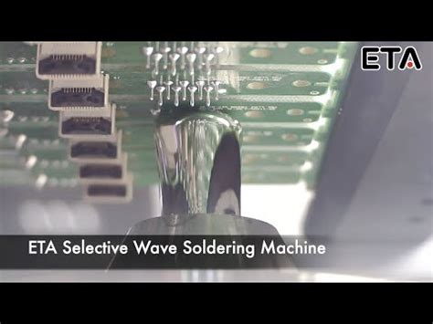
Wave Soldering
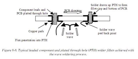
Wave soldering is a popular method for soldering through-hole components onto a PCB. It involves passing the board over a wave of molten solder, which flows up through the holes in the board and creates a connection between the component leads and the copper pads on the board.
Advantages of Wave Soldering
Wave soldering has several advantages over other soldering methods:
- It is a fast and automated process, which makes it suitable for high-volume production runs.
- It is capable of soldering multiple components simultaneously, which reduces assembly time and cost.
- It produces a consistent and reliable solder joint, which improves the overall quality of the finished board.
Wave Soldering Process
The wave soldering process involves several steps:
-
Fluxing: The board is first coated with a layer of flux, which helps to remove oxides from the metal surfaces and promotes wetting of the solder.
-
Preheating: The board is then passed through a preheating zone, which raises the temperature of the board and components to just below the melting point of the solder. This helps to prevent thermal shock and reduces the risk of component damage.
-
Soldering: The board is then passed over a wave of molten solder, which is typically a mixture of tin, lead, and other metals. The solder wave is generated by a pump that forces the molten solder up through a nozzle and onto the board. As the board passes over the wave, the molten solder flows up through the holes in the board and creates a connection between the component leads and the copper pads.
-
Cooling: After soldering, the board is passed through a cooling zone, which allows the solder joints to solidify and cool down gradually to prevent thermal stress.
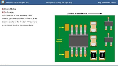
Designing for Wave Soldering
To ensure a successful wave soldering process, the PCB design must be optimized for the process. Some key considerations include:
-
Component orientation: Components should be oriented in the same direction as the direction of travel of the board through the solder wave. This helps to prevent shadowing and ensures that all components are properly soldered.
-
Solder thieves: Solder thieves are large copper pads placed near the edges of the board that help to draw excess solder away from the components and prevent bridging.
-
Thermal relief: Thermal relief pads are used to connect large copper areas, such as ground planes, to the component pads. These pads have a reduced copper area, which helps to prevent heat from being drawn away from the component during soldering.
Limitations of Wave Soldering
While wave soldering is a highly effective method for soldering through-hole components, it does have some limitations:
- It is not suitable for surface mount components, which require a different soldering method, such as reflow soldering.
- It can be difficult to solder components with very small lead spacing or those that are sensitive to heat, such as certain types of capacitors or crystals.
- It requires careful design and preparation to ensure that the components are properly oriented and spaced for the soldering process.
Testing and Inspection
Once the assembly process is complete, the board must be tested and inspected to ensure that it is functioning correctly and meets the required specifications. There are several methods for testing and inspecting PCBs:
-
Visual inspection: The board is visually inspected for any obvious defects, such as missing components, short circuits, or solder bridges.
-
Automated optical inspection (AOI): AOI uses computer vision to automatically inspect the board for defects and ensure that all components are properly placed and soldered.
-
Electrical testing: The board is tested for electrical continuity and functionality using specialized equipment, such as a multimeter or oscilloscope.
-
Functional testing: The board is tested under real-world conditions to ensure that it performs as expected and meets the required specifications.
Conclusion
PCB manufacturing is a complex process that involves several steps, from design and fabrication to assembly and testing. Wave soldering is a critical step in the assembly process, particularly for through-hole components, and requires careful design and preparation to ensure a successful outcome.
By understanding the various processes involved in PCB manufacturing and the specific requirements of wave soldering, designers and manufacturers can optimize their designs and processes to produce high-quality, reliable PCBs that meet the needs of their customers.
Frequently Asked Questions
What is the difference between wave soldering and reflow soldering?
Wave soldering is used for soldering through-hole components, while reflow soldering is used for surface mount components. Wave soldering involves passing the board over a wave of molten solder, while reflow soldering involves applying solder paste to the board and then heating it in an oven to melt the solder and create a connection.
Can wave soldering be used for surface mount components?
Wave soldering is not typically used for surface mount components, as the small size and close spacing of the components makes it difficult to create a reliable solder joint. Surface mount components are typically soldered using reflow soldering or other specialized methods.
What is the purpose of the solder mask on a PCB?
The solder mask is a protective layer that covers the copper traces on the PCB, leaving only the areas where components will be soldered exposed. This helps to prevent short circuits and makes the soldering process easier by preventing solder from flowing where it is not needed.
How can I optimize my PCB design for wave soldering?
To optimize your PCB design for wave soldering, you should consider factors such as component orientation, solder thieves, and thermal relief pads. Components should be oriented in the same direction as the direction of travel of the board through the solder wave, and solder thieves and thermal relief pads can help to prevent excess solder and heat from damaging the components.
What are some common defects that can occur during wave soldering?
Some common defects that can occur during wave soldering include bridging (where solder flows between adjacent pads), insufficient solder (where there is not enough solder to create a reliable connection), and damaged components (where the heat from the solder wave damages sensitive components). Careful design and process control can help to minimize these defects and ensure a high-quality finished board.
Leave a Reply