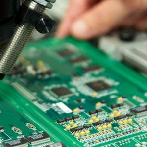
The Importance of PCBs in Modern Electronics
PCBs are the backbone of modern electronics, providing the platform for interconnecting electronic components and enabling the functionality of devices. They are used in a wide range of applications, from consumer electronics and automotive systems to aerospace and medical devices. The PCB industry plays a crucial role in the development and manufacturing of these boards, ensuring they meet the required specifications and standards.
The Growth of the PCB Industry
The PCB industry has experienced steady growth over the past few decades. According to a report by Grand View Research, the global PCB market size was valued at USD 60.2 billion in 2020 and is expected to expand at a compound annual growth rate (CAGR) of 4.3% from 2021 to 2028. This growth can be attributed to the increasing demand for electronic devices, the rise of the Internet of Things (IoT), and the advancements in 5G technology.
| Year | Market Size (USD Billion) |
|---|---|
| 2020 | 60.2 |
| 2028 | 85.7 (projected) |
Table 1: Global PCB Market Size Growth
Technological Challenges in the PCB Industry
Despite the growth and advancements in the PCB industry, manufacturers face several technological challenges that must be addressed to meet the evolving demands of the market.
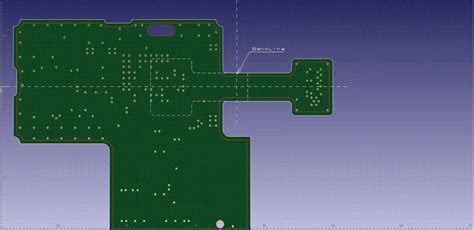
Miniaturization and High Density Interconnect (HDI)
One of the primary challenges in the PCB industry is the trend towards miniaturization and the need for High Density Interconnect (HDI) PCBs. As electronic devices become smaller and more compact, PCBs must follow suit. HDI PCBs feature finer traces, smaller vias, and higher layer counts, allowing for greater component density and improved performance.
However, manufacturing HDI PCBs presents several challenges, such as:
- Maintaining precise trace widths and spacings
- Drilling small, high-aspect-ratio vias
- Ensuring proper registration between layers
- Controlling impedance and signal integrity
To overcome these challenges, PCB manufacturers must invest in advanced equipment, such as high-precision laser drills and direct imaging systems. Additionally, the use of materials with improved electrical and thermal properties, such as low-loss dielectrics and high-conductivity copper, can help mitigate signal integrity issues.
Materials and Substrate Selection
The selection of appropriate materials and substrates is crucial for the performance and reliability of PCBs. With the increasing demands for high-speed, high-frequency, and high-temperature applications, PCB manufacturers must carefully choose materials that can withstand these conditions.
Some challenges related to materials and substrate selection include:
- Ensuring compatibility between different materials
- Managing the coefficient of thermal expansion (CTE) mismatch
- Maintaining dielectric constant and loss tangent values
- Addressing the need for lead-free and halogen-free materials
To overcome these challenges, PCB manufacturers must collaborate closely with material suppliers to develop and qualify new materials that meet the specific requirements of their applications. The use of advanced simulation tools and material characterization techniques can help predict the behavior of materials under various conditions and optimize the design accordingly.
Signal Integrity and Power Integrity
As the speed and frequency of electronic devices increase, maintaining signal integrity and power integrity becomes increasingly challenging. Signal integrity issues, such as crosstalk, reflections, and electromagnetic interference (EMI), can lead to data corruption and system failures. Power integrity issues, such as voltage drops and ground bounces, can cause performance degradation and reliability problems.
To address these challenges, PCB designers must employ various techniques, such as:
- Proper grounding and shielding
- Impedance matching and termination
- Decoupling and bypass capacitors
- Careful routing and layer stackup design
Additionally, the use of advanced simulation tools, such as 3D electromagnetic (EM) solvers and power integrity analyzers, can help identify and mitigate potential issues early in the design process.
Thermal Management
With the increasing power densities and heat generation in electronic devices, thermal management has become a critical challenge in the PCB industry. Inadequate thermal management can lead to component failures, reduced reliability, and shorter product lifespans.
PCB manufacturers must employ various thermal management techniques to overcome this challenge, such as:
- Using high-thermal-conductivity materials, such as metal-core PCBs and thermal vias
- Incorporating heatsinks and heat spreaders
- Optimizing component placement and airflow
- Employing active cooling methods, such as fans and liquid cooling systems
The use of thermal simulation tools can help predict the temperature distribution across the PCB and identify potential hot spots, allowing designers to optimize the thermal design accordingly.
Manufacturing Process Control and Quality Assurance
Ensuring consistent quality and reliability is a significant challenge in the PCB manufacturing process. With the increasing complexity of PCBs and the tighter tolerances required, manufacturers must implement strict process control and quality assurance measures.
Some challenges related to manufacturing process control and quality assurance include:
- Maintaining tight tolerances for trace widths, spacings, and via sizes
- Ensuring proper registration and alignment between layers
- Controlling the plating process for consistent thickness and adhesion
- Detecting and preventing defects, such as shorts, opens, and voids
To overcome these challenges, PCB manufacturers must invest in advanced process control equipment, such as automated optical inspection (AOI) systems and 3D X-ray inspection machines. The implementation of statistical process control (SPC) and Six Sigma methodologies can help identify and eliminate sources of variation in the manufacturing process.
Strategies for Overcoming PCB Challenges
To overcome the technological challenges in the PCB industry, manufacturers and designers must adopt a multi-faceted approach that involves collaboration, innovation, and continuous improvement.
Collaboration and Communication
Effective collaboration and communication between PCB manufacturers, designers, and end-users are essential for addressing the challenges in the industry. By fostering open dialogue and sharing knowledge and expertise, stakeholders can work together to identify and solve problems more efficiently.
Some strategies for improving collaboration and communication include:
- Establishing regular meetings and workshops to discuss challenges and share best practices
- Using collaborative design tools and platforms to facilitate real-time communication and feedback
- Implementing a formal design review process to ensure all stakeholders are aligned on requirements and specifications
Investment in Research and Development
To stay ahead of the curve and address the ever-evolving challenges in the PCB industry, manufacturers must invest in research and development (R&D). By dedicating resources to developing new materials, processes, and technologies, manufacturers can drive innovation and create competitive advantages.
Some areas of focus for R&D in the PCB industry include:
- Advanced materials, such as graphene and carbon nanotubes
- 3D printing and additive manufacturing technologies
- High-frequency and high-speed design techniques
- Artificial intelligence and machine learning for process optimization and quality control
Adoption of Industry 4.0 Technologies
Industry 4.0, also known as the Fourth Industrial Revolution, refers to the integration of advanced technologies, such as the Internet of Things (IoT), big data analytics, and artificial intelligence, into manufacturing processes. By adopting these technologies, PCB manufacturers can improve efficiency, reduce costs, and enhance quality control.
Some examples of Industry 4.0 technologies in the PCB industry include:
- Smart factories with connected machines and sensors for real-time monitoring and control
- Predictive maintenance using machine learning algorithms to anticipate and prevent equipment failures
- Automated visual inspection systems using deep learning for defect detection and classification
- Digital twins for virtual prototyping and process optimization

Frequently Asked Questions (FAQ)
-
What is the biggest challenge facing the PCB industry today?
The biggest challenge facing the PCB industry today is the trend towards miniaturization and the need for High Density Interconnect (HDI) PCBs. As electronic devices become smaller and more compact, PCBs must follow suit, which presents several manufacturing challenges, such as maintaining precise trace widths and spacings, drilling small vias, and ensuring proper registration between layers. -
How can PCB manufacturers ensure signal integrity in high-speed applications?
To ensure signal integrity in high-speed applications, PCB manufacturers must employ various techniques, such as proper grounding and shielding, impedance matching and termination, and the use of decoupling and bypass capacitors. Additionally, careful routing and layer stackup design, along with the use of advanced simulation tools, can help identify and mitigate potential signal integrity issues early in the design process. -
What are some thermal management techniques used in PCBs?
Some thermal management techniques used in PCBs include the use of high-thermal-conductivity materials (such as metal-core PCBs and thermal vias), incorporating heatsinks and heat spreaders, optimizing component placement and airflow, and employing active cooling methods, such as fans and liquid cooling systems. -
How can collaboration and communication help address PCB challenges?
Effective collaboration and communication between PCB manufacturers, designers, and end-users can help address challenges by fostering open dialogue and sharing knowledge and expertise. This can be achieved through regular meetings and workshops, the use of collaborative design tools and platforms, and the implementation of a formal design review process. -
What role does research and development play in overcoming PCB challenges?
Research and development (R&D) plays a crucial role in overcoming PCB challenges by driving innovation and creating competitive advantages. By investing in R&D and focusing on areas such as advanced materials, 3D printing, high-frequency design techniques, and artificial intelligence, PCB manufacturers can develop new solutions to address the ever-evolving challenges in the industry.
Conclusion
The PCB industry faces numerous technological challenges, from miniaturization and high-density interconnects to signal integrity and thermal management. To overcome these challenges, manufacturers and designers must adopt a multi-faceted approach that involves collaboration, innovation, and continuous improvement.
By investing in research and development, adopting Industry 4.0 technologies, and fostering effective communication and collaboration, the PCB industry can continue to drive advancements in electronic devices and meet the evolving demands of the market. As the industry continues to grow and evolve, it is essential for stakeholders to remain proactive and adaptable in the face of new challenges and opportunities.
Leave a Reply