What is PCB Design Software?
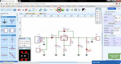
PCB design software, also known as printed Circuit Board design software or electronic design automation (EDA) software, is a specialized computer-aided design (CAD) tool used to create and edit layouts for printed circuit boards. These software packages allow engineers and designers to develop complex PCB layouts, from schematic capture to final board layout and manufacturing files.
Key Features of PCB Design Software
-
Schematic Capture: This feature allows designers to create a visual representation of the electronic circuit using symbols and connections.
-
Component Libraries: PCB design software includes extensive libraries of electronic components, which can be placed on the board layout.
-
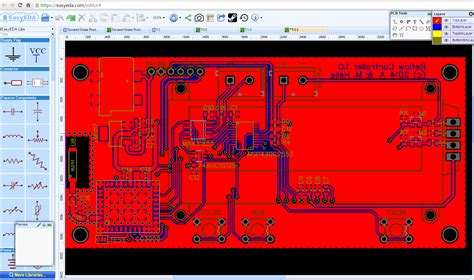
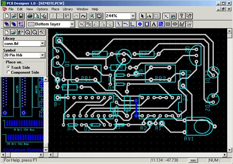
Board Layout: The software provides tools for placing components, routing traces, and defining board boundaries.
-
Design Rule Checking (DRC): Automated checks ensure that the PCB layout adheres to manufacturing and electrical constraints.
-
3D Visualization: Many PCB design software packages offer 3D rendering capabilities, allowing designers to visualize the final board assembly.
Popular PCB Design Software Packages
There are several commercial and open-source PCB design software options available in the market. Some of the most popular ones include:
| Software | Vendor | Key Features |
|---|---|---|
| Altium Designer | Altium | Comprehensive PCB design suite with advanced features for high-speed designs |
| EAGLE | Autodesk | User-friendly interface, extensive component libraries, and affordable pricing |
| KiCad | Open Source | Free and open-source, supporting schematic capture, PCB layout, and 3D visualization |
| OrCAD | Cadence | Industry-standard tool with advanced simulation and analysis capabilities |
| PADS | Mentor Graphics | Scalable solution for PCB design, from entry-level to advanced high-speed designs |
The PCB Design Process
The PCB design process typically involves several stages, each requiring specific features of the PCB design software.
1. Schematic Capture
The first step in PCB design is creating a schematic diagram, which represents the electrical connections between components. PCB design software provides a schematic capture tool, allowing designers to place component symbols and define their connections using nets or wires.
2. Component Placement
Once the schematic is complete, the next step is to place the components on the PCB layout. The software’s component libraries contain footprints for various electronic components, which can be placed on the board and arranged for optimal performance and manufacturability.
3. Board Routing
After component placement, the designer must route the traces between the components according to the schematic’s electrical connections. PCB design software provides manual and automated routing tools to create efficient and reliable connections while adhering to design rules and constraints.
4. Design Rule Checking
Throughout the PCB design process, the software continuously checks the layout against a set of predefined design rules to ensure that it meets manufacturing and electrical requirements. These checks help identify and resolve issues related to trace widths, clearances, and other critical parameters.
5. Output Generation
Once the PCB layout is complete and has passed the design rule checks, the software generates output files for manufacturing. These files typically include Gerber files, drill files, and bill of materials (BOM), which are sent to the PCB fabrication and assembly houses.

Advantages of Using PCB Design Software
Using PCB design software offers several advantages over manual PCB design methods:
-
Increased Efficiency: PCB design software automates many tasks, such as component placement and routing, significantly reducing design time and effort.
-
Improved Accuracy: Automated design rule checks and built-in constraints help ensure that the PCB layout is error-free and manufacturable.
-
Enhanced Collaboration: Many PCB design software packages support version control and collaborative design, allowing team members to work on the same project simultaneously.
-
Cost Savings: By streamlining the design process and minimizing errors, PCB design software helps reduce overall development costs and time-to-market.
-
Flexibility and Scalability: PCB design software adapts to various project requirements, from simple single-layer boards to complex multi-layer designs with high-speed constraints.
Choosing the Right PCB Design Software
When selecting a PCB design software package, consider the following factors:
-
Project Requirements: Evaluate the complexity of your PCB designs and ensure that the software can handle your specific requirements, such as high-speed design, multi-layer boards, or advanced simulation capabilities.
-
User Interface and Learning Curve: Consider the software’s ease of use and the availability of learning resources, such as tutorials, documentation, and user communities.
-
Integration and Compatibility: Ensure that the PCB design software integrates well with your existing tools and workflows, such as mechanical CAD software or version control systems.
-
Cost and Licensing: Compare the costs of different software packages, considering factors such as perpetual licenses, subscription models, and the availability of free or open-source alternatives.
-
Customer Support and Updates: Evaluate the level of customer support provided by the software vendor and the frequency of software updates and new feature releases.
Frequently Asked Questions (FAQ)
1. Is PCB design software necessary for creating printed circuit boards?
While it is possible to design simple PCBs manually, using PCB design software is highly recommended for most projects. The software streamlines the design process, reduces errors, and ensures that the final board layout is manufacturable and meets industry standards.
2. Can I use PCB design software without prior experience in electronic design?
Many PCB design software packages offer user-friendly interfaces and extensive learning resources, making it possible for beginners to start designing PCBs. However, a basic understanding of electronic circuits and PCB manufacturing processes is highly beneficial.
3. Are there any free or open-source PCB design software options available?
Yes, there are several free and open-source PCB design software packages available, such as KiCad and FreePCB. These tools offer a wide range of features and are suitable for many PCB design projects.
4. Can PCB design software be used for high-speed or RF designs?
Advanced PCB design software packages, such as Altium Designer and OrCAD, offer specialized features for high-speed and RF designs, including signal integrity analysis, impedance matching, and electromagnetic simulation capabilities.
5. How do I choose the right PCB design software for my project?
When selecting PCB design software, consider factors such as your project requirements, the software’s ease of use, integration with existing tools, cost, and customer support. It’s also helpful to evaluate free trials or demo versions of different software packages to find the one that best suits your needs.
Conclusion
PCB design software is an essential tool for creating printed circuit boards efficiently and accurately. By automating tasks, providing extensive component libraries, and ensuring adherence to design rules, these software packages streamline the PCB design process and help engineers and designers bring their electronic projects to life.
When choosing a PCB design software package, consider your project requirements, budget, and the software’s ease of use. With the right tools and a solid understanding of the PCB design process, you can create high-quality, manufacturable PCBs that meet your specific needs.
Leave a Reply