What is Solder Mask and Why is it Important?
Solder mask, also known as solder resist or solder stop mask, is a thin layer of polymer that is applied to the copper traces of a printed circuit board (PCB). The primary purpose of solder mask is to protect the copper traces from oxidation, prevent solder bridges from forming between closely spaced pads, and provide electrical insulation.
Solder mask plays a crucial role in the manufacturing and assembly of PCBs. It offers several benefits:
-
Protection against oxidation: Copper traces on a PCB can easily oxidize when exposed to air, leading to reduced conductivity and potential circuit failures. Solder mask acts as a barrier, preventing oxygen from reaching the copper surface.
-
Solder bridge prevention: During the soldering process, molten solder can inadvertently connect adjacent pads or traces, creating short circuits. Solder mask covers the areas where solder should not adhere, minimizing the risk of solder bridges.
-
Electrical insulation: Solder mask provides electrical insulation between copper traces, preventing unintended connections and improving the overall reliability of the PCB.
-
Improved aesthetics: Solder mask is available in various colors, with green being the most common. It gives the PCB a clean and professional appearance, enhancing its visual appeal.
-
Identification and labeling: Solder mask can be used to print text, logos, or other identifying information on the PCB, making it easier to track and identify the board during manufacturing and assembly.
Solder Mask Application Methods
There are several methods used to apply solder mask to PCBs, each with its own advantages and limitations. The choice of method depends on factors such as the desired accuracy, production volume, and cost. The most common solder mask application methods are:
- Screen Printing
- Liquid Photo Imageable (LPI) Solder Mask
- Dry Film Solder Mask
Screen Printing
Screen printing is a traditional and widely used method for applying solder mask to PCBs. It involves using a fine mesh screen with a stencil of the desired solder mask pattern. The solder mask ink is pushed through the screen onto the PCB surface using a squeegee.
The screen printing process consists of the following steps:
-
Screen preparation: A fine mesh screen, typically made of polyester or stainless steel, is coated with a light-sensitive emulsion. The desired solder mask pattern is then exposed onto the emulsion, hardening the exposed areas.
-
Ink preparation: The solder mask ink is mixed and loaded onto the screen. The ink is usually a two-part epoxy or UV-curable polymer.
-
Printing: The PCB is placed beneath the screen, and the ink is applied using a squeegee. The squeegee is dragged across the screen, forcing the ink through the open areas of the stencil and onto the PCB surface.
-
Curing: After printing, the solder mask ink is cured using heat or UV light, depending on the type of ink used. Curing hardens the solder mask and ensures proper adhesion to the PCB.
| Pros | Cons |
|---|---|
| Cost-effective for low to medium volumes | Lower resolution compared to other methods |
| Simple and straightforward process | Potential for human error during printing |
| Suitable for various solder mask types | Limited ability to achieve fine details |
| Fast setup and changeover times | Requires frequent screen cleaning and maintenance |
Liquid Photo Imageable (LPI) Solder Mask
Liquid Photo Imageable (LPI) solder mask, also known as photoimageable solder mask or liquid photoimageable mask, is a high-resolution method for applying solder mask to PCBs. LPI solder mask is applied as a liquid coating and then selectively exposed and developed to create the desired pattern.
The LPI solder mask application process involves the following steps:
-
Surface preparation: The PCB surface is cleaned and treated to ensure proper adhesion of the solder mask.
-
Coating: The liquid solder mask is applied to the PCB surface using various methods, such as curtain coating, spray coating, or roller coating. The coating thickness is precisely controlled to ensure uniform coverage.
-
Prebaking: The coated PCB is prebaked to partially cure the solder mask and remove any solvents.
-
Exposure: The prebaked PCB is exposed to UV light through a photomask or phototool, which contains the desired solder mask pattern. The UV light hardens the exposed areas of the solder mask.
-
Developing: The unexposed areas of the solder mask are removed using a chemical developer, leaving behind the hardened solder mask pattern.
-
Final curing: The developed PCB undergoes a final curing process, usually in an oven, to fully crosslink and harden the solder mask.
| Pros | Cons |
|---|---|
| High resolution and accuracy | Higher cost compared to screen printing |
| Excellent ability to achieve fine details | Longer processing time |
| Uniform coating thickness | Requires specialized equipment |
| Suitable for high-volume production | Sensitivity to environmental conditions during processing |
Dry Film Solder Mask
Dry film solder mask is a solid photoresist film that is laminated onto the PCB surface and then exposed and developed to create the desired solder mask pattern. This method offers a balance between the simplicity of screen printing and the high resolution of LPI solder mask.
The dry film solder mask application process consists of the following steps:
-
Surface preparation: The PCB surface is cleaned and treated to ensure proper adhesion of the dry film.
-
Lamination: The dry film solder mask is laminated onto the PCB surface using heat and pressure. The lamination process ensures a strong bond between the film and the PCB.
-
Exposure: The laminated PCB is exposed to UV light through a photomask or phototool, which contains the desired solder mask pattern. The UV light crosslinks and hardens the exposed areas of the film.
-
Developing: The unexposed areas of the dry film are removed using a chemical developer, leaving behind the hardened solder mask pattern.
-
Final curing: The developed PCB undergoes a final curing process, usually in an oven, to fully crosslink and harden the solder mask.
| Pros | Cons |
|---|---|
| Good resolution and accuracy | Higher cost compared to screen printing |
| Uniform coating thickness | Limited flexibility in design changes |
| Less sensitive to environmental conditions | Requires specialized lamination equipment |
| Faster processing compared to LPI solder mask | Potential for air bubbles or wrinkles during lamination |
Solder Mask Color Options
Solder mask is available in a variety of colors, with each color serving a specific purpose or providing a unique aesthetic appeal. The most common solder mask colors are:
-
Green: Green is the most widely used solder mask color in the PCB industry. It provides good contrast against the copper traces and is easily recognizable as a PCB.
-
Blue: Blue solder mask is gaining popularity due to its high contrast against white silkscreen markings and its visually appealing appearance.
-
Red: Red solder mask is often used for high-visibility applications or to indicate special features on a PCB.
-
Black: Black solder mask offers a sleek and professional look, making it popular for consumer electronics and high-end devices.
-
White: White solder mask is less common but can be used for specific applications or to create a unique visual effect.
-
Yellow: Yellow solder mask is sometimes used for prototyping or to distinguish specific areas on a PCB.
The choice of solder mask color depends on factors such as industry standards, visual appeal, and the specific requirements of the end application.

Solder Mask Finish Options
In addition to color options, solder mask can be applied with different surface finishes to enhance the PCB’s performance or appearance. The most common solder mask finishes are:
-
Glossy: A glossy finish provides a smooth and shiny surface, making it easier to clean and inspect the PCB. However, it can be prone to glare and reflections.
-
Matte: A matte finish offers a non-reflective surface that minimizes glare and improves readability of silkscreen markings. It also provides a better surface for adhesive labels or stickers.
-
Semi-glossy: A semi-glossy finish strikes a balance between the glossy and matte finishes, offering a slightly reflective surface with reduced glare.
The choice of solder mask finish depends on the specific requirements of the PCB, such as the need for easy cleaning, improved readability, or a particular aesthetic appearance.
Solder Mask Thickness and Coverage
The thickness and coverage of solder mask are critical factors in ensuring proper protection and insulation of the PCB. The ideal solder mask thickness depends on the application method and the specific requirements of the PCB.
| Application Method | Typical Thickness Range |
|---|---|
| Screen Printing | 0.0005″ – 0.002″ |
| LPI Solder Mask | 0.0008″ – 0.002″ |
| Dry Film Solder Mask | 0.0015″ – 0.003″ |
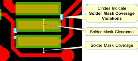
Solder mask coverage is usually specified in terms of the minimum distance between the edge of the solder mask opening and the adjacent copper feature. This distance is known as the solder mask clearance or solder mask expansion. The solder mask clearance ensures that the copper pads are exposed for soldering while providing adequate insulation between adjacent features.
The solder mask clearance is typically specified in the PCB design files and can range from 0.003″ to 0.01″ or more, depending on the PCB layout and the manufacturing capabilities of the PCB fabricator.
Solder Mask Inspection and Quality Control
Ensuring the quality and integrity of the solder mask is crucial for the reliability and performance of the PCB. Several inspection and quality control methods are used to verify the solder mask application:
-
Visual inspection: A visual examination of the PCB is performed to check for any defects, such as pinholes, blisters, or incomplete coverage. This inspection is usually done using a magnifying lens or microscope.
-
Thickness measurement: The thickness of the solder mask is measured using a thickness gauge or micrometer to ensure that it meets the specified requirements.
-
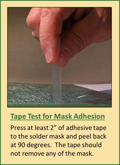
Adhesion testing: The adhesion of the solder mask to the PCB surface is tested using a tape test or cross-hatch test. These tests involve applying and removing a piece of tape or making a series of cuts in the solder mask and checking for any peeling or lifting.
-
Electrical testing: Electrical tests, such as insulation resistance and dielectric withstanding voltage tests, are performed to verify the insulating properties of the solder mask.
-
Contamination testing: The solder mask is tested for ionic contamination using a solvent extract test or a resistivity of solvent extract (ROSE) test. These tests ensure that the solder mask does not contain any ionic contaminants that could lead to corrosion or electrical failures.
By conducting thorough inspections and quality control measures, PCB manufacturers can ensure that the solder mask meets the required specifications and provides adequate protection for the PCB.
Frequently Asked Questions (FAQ)
-
What is the purpose of solder mask on a PCB?
Solder mask serves several purposes on a PCB, including protecting the copper traces from oxidation, preventing solder bridges from forming between closely spaced pads, providing electrical insulation, and improving the overall aesthetics of the board. -
What are the most common solder mask application methods?
The most common solder mask application methods are screen printing, liquid photo imageable (LPI) solder mask, and dry film solder mask. Each method has its own advantages and limitations, and the choice depends on factors such as desired accuracy, production volume, and cost. -
What is the most common color for solder mask?
Green is the most widely used solder mask color in the PCB industry. It provides good contrast against the copper traces and is easily recognizable as a PCB. However, other colors such as blue, red, black, white, and yellow are also available for specific applications or aesthetic purposes. -
How thick is solder mask typically applied?
The thickness of solder mask varies depending on the application method. Screen printing typically results in a thickness range of 0.0005″ to 0.002″, while LPI solder mask ranges from 0.0008″ to 0.002″, and dry film solder mask ranges from 0.0015″ to 0.003″. -
What quality control measures are used to ensure the integrity of the solder mask?
Several quality control measures are used to ensure the integrity of the solder mask, including visual inspection for defects, thickness measurement, adhesion testing, electrical testing for insulation properties, and contamination testing for ionic contaminants. These measures help ensure that the solder mask meets the required specifications and provides adequate protection for the PCB.
By understanding the importance of solder mask, the various application methods, and the quality control measures involved, PCB designers and manufacturers can ensure that their boards are properly protected and function reliably in their intended applications.
Leave a Reply