High frequency printed circuit boards (PCBs) are designed to operate at high frequencies, typically in the RF (radio frequency) and microwave bands from 300 MHz to 300 GHz. They enable the transmission of high frequency signals in devices and components used for wireless communications, radars, satellite equipment, medical devices and test equipment among others.
The critical considerations when designing high frequency PCBs include impedance control, loss control, cross-talk minimization and radiation control. Advanced design principles must be used to address signal integrity issues encountered at high operating frequencies. Special materials, manufacturing processes and testing are required to fabricate these specialized boards.
Applications of High Frequency PCBs
- Wireless communications infrastructure – base stations, routers, backhaul
- Radar and defense electronics
- Satellite communications
- Medical devices – MRI machines
- Automotive electronics – collision detection systems
- Testing equipment – signal generators, spectrum analyzers, network analyzers
Challenges with High Frequency PCB Design
The major design challenges stem from the increased sensitivity of signals at higher frequencies.
- Impedance control – signals require a specified controlled impedance environment to propagate without reflections.
- Loss and attenuation control – high frequencies see more loss in dielectric and conductors
- Cross-talk – high frequency agility leads to interfering signals coupling between traces
- Radiation and EMI control – tendency for signals to radiate as antennas
High Frequency PCB Materials
The materials used determine much of the performance capabilities of a high frequency PCB. Key considerations are dielectric constant, loss tangent and thermal properties.
Dielectric Materials
The dielectric material separates and supports the conductors. Key properties:
- Dielectric constant (Dk) – governs impedance and propagation velocity
- Loss tangent (Df) – causes signal loss and attenuation
- Common high frequency materials:
- PTFE (Dk = 2.2)
- Ceramic filled PTFE (lower Dk)
- Woven fiberglass (Dk = 3-4)
| Material | Dielectric Constant | Loss Tangent |
|---|---|---|
| PTFE | 2.2 | 0.001 |
| Ceramic filled PTFE | 3-10 | 0.002-0.005 |
| FR4 (fiberglass) | 4.5 | 0.02 |
- Low Dk, low Df materials are optimal but expensive
- Composite materials aim for optimal tradeoffs
Conductor Materials
The conductors carry high frequency signals between components:
- Copper is the standard – high conductivity
- Copper thickness – 1⁄2 to 2 oz typical for good conduction
- Plated finishes determine solderability and shelf life
- HASL, ENIG, Immersion Silver
- Mixed material approaches
- Copper conductors with composite dielectric
Substrate Materials
The substrate is the base layer that copper layers are built on:
- Tempered glass – extremely stable, low loss
- Ceramic substrates – high stability, good thermal performance
- Laminates – glass or ceramic reinforced resin sheets
High Frequency PCB Design Principles
Applying appropriate design principles is key to mitigating loss, reflection, cross-talk and radiation issues.
Controlled Impedance
- Match PCB trace impedance to source, load impedance (often 50 Ohms)
- Achieved by width/height ratio of traces
- Both signal and return path must have controlled impedance
Minimize Stubs
- Stubs cause impedance discontinuities leading to reflections
- Keep lines short or use mitered corners to connect
- Use termination resistors and capacitors to dampen effects
Bypassing and Decoupling
- Use capacitors near integrated circuits to provide charge reservoirs
- Reduce power supply noise – important for fast switching digital logic
Maintain Signal Symmetry
- Equal line lengths, matched components for differential pairs
- Minimize skew between lengths to reduce interference
- Facilitates high speed communication
Route Signals Efficiently
- Use 45 degree angles rather than 90 degree bends
- Avoid sharp corners which cause discontinuities
- Changes in direction should be gradual
High Frequency PCB Manufacturing
Specialized processes required to produce high frequency circuit boards.
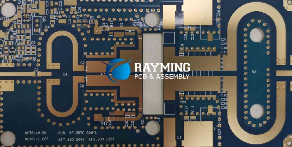
Stackup Construction <h3>
- Layers designed to inhibit cross-talk
- Ground and power planes shield signals
- Number of layers accommodate complexity
- 4-16+ layers common for high frequency designs
Registration Accuracy
- Consistent alignment across layers
- Ensures impedance control, reliable connections
- Requires advanced equipment and processes
Controlled Dielectric Thickness
- Conductor widths tuned for target Dk and trace height
- Consistent dielectric thickness vital
- Achieved by lamination, press cycles, and polishing
Hole Plating Quality
- Full copper plating of drilled vias
- Ensures conduction through layers
- Specialized plating processes employed
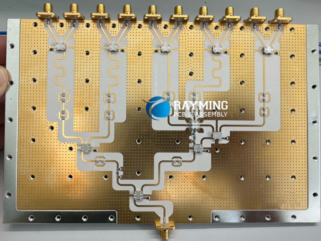
Fine Line Capability
- High density designs need tight trace spacing
- Line widths down to 3 mils (0.15mm) achieved
Testing
- Electrical testing
- Verify controlled impedance transmission lines
- RF/signal integrity testing
- Time-domain reflectometry
- Return/insertion loss measurements
Cost Factors for High Frequency PCBs
What drives cost for these specialized boards?
Materials Cost
- Base dielectric and conductor materials
- PTFE and ceramic dielectrics more expensive
- Thick copper, final metal platings add cost
Design Complexity
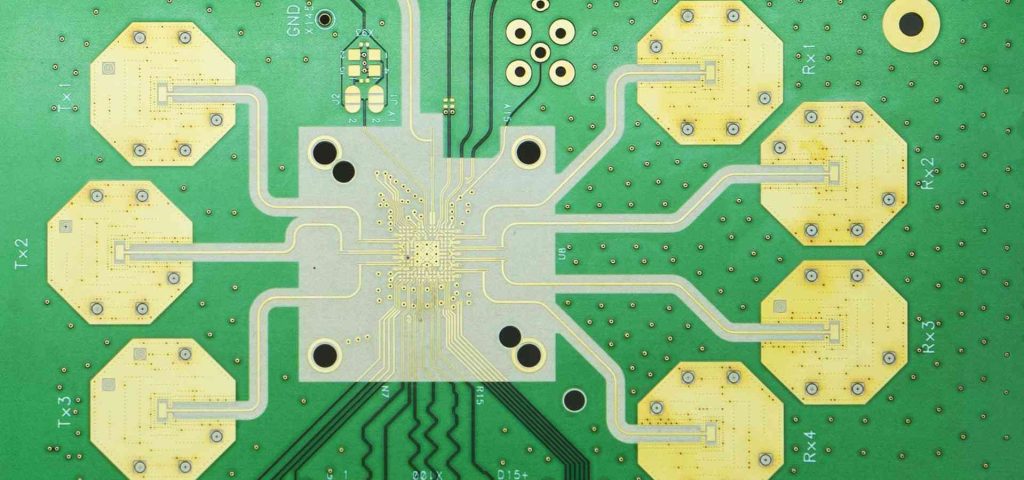
- Component density – fine features, small spacings
- Layer count – 8+ layers typical
- Blind and buried vias needed – complex lamination
Testing and Validation
- Impedance and signal integrity testing requires equipment investment
- Iterations to verify performance increase cost
Low Volume Production
- High frequency boards often used in lower quantities
- Limits manufacturing efficiency benefits
Certification Requirements
- Some applications demand rigorous quality control
- Defense, aerospace, medical industries in particular
- Certifications become barriers to entry impacting supply
High Frequency PCB Design & Manufacturing – FAQs
What are some key considerations when selecting materials?
When selecting PCB substrate and dielectric materials for high frequency applications, low dielectric constant (Dk) and low loss tangent (Df) are typically desired. This helps minimize signal loss and reflection issues. Composite materials aim to balance cost with acceptable electrical properties and thermal characteristics.
What construction techniques help reduce cross-talk?
Using ground planes between signals layers, routing signals orthogonally between layers, interspersing ground traces between signals on a layer, and maintaining symmetry across differential pairs helps mitigate cross-talk issues. Shielding around critical traces may also be used.
Why is impedance control important?
Controlling characteristic impedance, typically to 50 Ohms, along transmission line PCB traces ensures proper impedance matching between source, transmission line and load impedance. This avoids signal reflections which corrupt signal integrity and cause erratic circuit operation at high frequencies.
What are some key PCB testing methods?
Time-domain reflectometry using special oscilloscopes is popular for verifying controlled impedance signal paths. This looks for discontinuities causing reflections. Insertion loss measurements determine signal loss through a trace. Power integrity, communications integrity and EMI testing may also be used to characterize high frequency board performance.
How does design complexity impact cost?
Denser designs with fine feature sizes, tighter tolerances, specialized via configurations and higher layer counts require more sophisticated PCB processes to produce. This demands specialized equipment and know-how, driving cost upward. Advanced testing also increases with complexity adding cost.
Leave a Reply