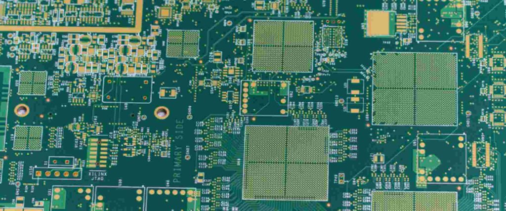
What is HDI PCB?
HDI (High-Density Interconnect) PCBs are printed circuit boards (PCBs) with a higher wiring density than conventional PCBs. HDI PCBs contain microvias – small vias with diameters under 0.15mm connecting two or more conductive layers. The use of microvias allows trace pitches under 8 mil, increasing circuit density.
HDI PCBs support high I/O density requirements for advanced IC packaging. They enable miniaturization and integration of multifunction electronics. HDI technology provides benefits like:
- Higher wiring densities
- More routing channels
- Smaller vias pads
- Thinner dielectric layers
- Reduced layer counts
With the continued trend towards device miniaturization and microelectronics, HDI PCBs have become essential in product design across industries like automotive, aerospace, medical, telecom, and consumer electronics.
HDI PCB Classification
HDI PCBs are classified based on the number of conductive layers and definitions of microvias:
1+N+1 HDI
This configuration has one signal layer on top and bottom. Multiple plane layers are embedded inside with microvias connecting them as required.
2+N+2 HDI
This configuration has two signal layers on top and bottom. Multiple plane layers are embedded inside with microvias connecting them as required.
| Configuration | Top Layer | Bottom Layer | Inner Layers |
|---|---|---|---|
| 1+N+1 HDI | Signal | Signal | Signal + Power/Ground |
| 2+N+2 HDI | Signal | Signal | Signal + Power/Ground |
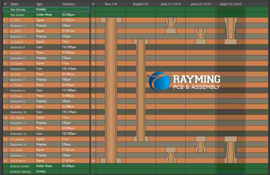
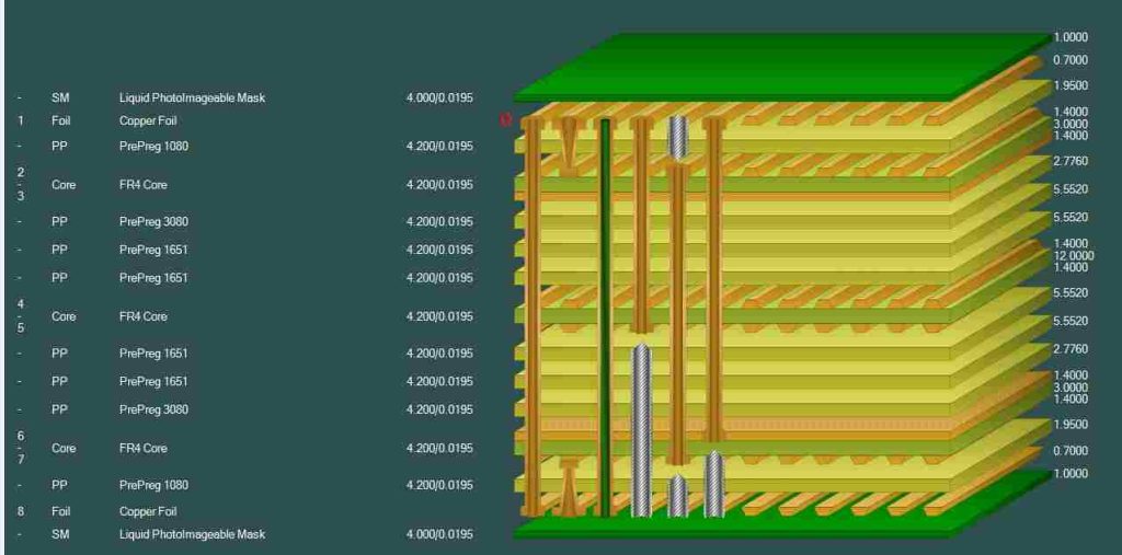
HDI PCB Architecture Overview
HDI PCB architecture includes the key components of dielectric materials, microvias, and trace/space.
Dielectric Layers
Dielectric layers electrically separate conductive copper layers in a PCB while holding the laminated stack together. Common rigid dielectric materials include:
- FR-4 Glass Epoxy
- Polyimide
- PTFE Composites
- Ceramics
- Others (BT resins, cyanate esters)
Flexible HDI PCBs use flexible dielectric films like polyimide (PI). The dielectric constant and loss tangent dictate electrical performance. Low Dk and Df are ideal.
With high functionality requirements, HDI PCB dielectric layers need:
- Thin profiles (~25μm)
- Good dimensional stability
- Low moisture absorption
- High glass transition temperatures
- Excellent chemical resistance
Microvias
Microvias in HDI PCBs have diameters under 150μm, allowing traces with sub-8 mil pitch. They electrically connect different layers passing through dielectric films. Based on the interconnect structure, common HDI microvia types are:
Blind Vias: Connecting outer layer(s) to inner layer(s)
Buried Vias: Interconnecting inner layers only (no connection to outer layers)
Stacked/Staggered Vias: Vertical interconnects through multiple layers
Buried and stacked vias allow layer fan-outs beneath components for routing high density traces.
Trace/Space
The trace refers to the copper conductor lines on a PCB layer. The space is the distance between adjacent trace centerlines.
Common trace/space dimensions for HDI PCBs per IPC-2226 standard:
| Trace Width | Space Width | Pitch |
|---|---|---|
| ≥ 0.1mm (4mil) | ≥ 0.1mm (4mil) | ≥ 0.2mm (8mil) |
Finer trace/space under 5 mil is possible with thin dielectrics and precise fab processes.
HDI PCB Design Rules
HDI PCB layout adheres to stringent design rules for reliability. Key rules govern trace width/space, microvia capture pads, and via placement.
Trace Width/Space
The minimum trace width and space depend on the layer location:
External Layers: Min width/space ≥ 4 mil
Internal Layers: Min width/space ≥ 3 mil
Narrower traces down to 2 mil are possible but need special consideration for current density. Analysis using IPC 2152 or simulation is recommended.
Microvia Capture Pad
Capture pad refers to the copper area surrounding a microvia. Different shapes are possible based on layer design.
External Layer Capture Pad: Circular or octagonal shape with ≥5 mil diameter
Internal Layer Capture Pad: Circular shape with ≥4 mil diameter
Adequate capture pads are essential to facilitate model continuity between layers and ensure the structural rigidity of microvias.
Microvia Placement
Microvia placement relative to the surrounding copper defines registration tolerance. Various placement options are:
- Centered (mid-land)
- Closer to conductor edge (toe-land)
- Under conductor (filled-land)
Toe-land and filled-land vias require more precision in drilling and metallic plating to avoid openings. Mid-land placement eases tolerances. IPC-2226A defines microvia placement requirements.
HDI PCB Layout Guidelines
Proper layout techniques are critical to harness the benefits of HDI PCBs effectively:
1. Group High Speed Traces: Signals with high edge rates should be routed together in bundles with ground fills separating bundles. This controlled impedance environment avoids EMI issues.
2. Use Gridded Power Planes: Solid power/ground planes should be gridded with isolation bands in HDI PCBs. Grids prevent plane cavities while improving current flow.
3. Define Stackup Early: Finalizing layer stack, dielectric materials, trace widths and microvia dimensions early is necessary. It impacts manufacturing process capability.
4. Follow Assembly Standards: Standards like IPC-2226/7351 for trace space/width, annular rings, and fabrication can assure quality and reliability.
5. Simulate Before Committing: Extensive simulation of HDI PCB stackup, routing, thermal performance, and signal integrity early in the design flow is highly recommended.
6. Manage Via Transitions: Any transition between conventional PTHs to blind/buried vias needs managing capacitance with ground vias or planes around the transition.
7. Watch Spacing tolerances: Use larger capture pads or relaxed microvia spacing on tighter space layers to ease registration issues during lamination.
8. Limit Aspect Ratios: Keep microvia aspect ratio (AR= height/diameter) under 10:1. High AR vias can cause reliability risks due to drill wander.
9. Follow IPC Guidelines: Guidelines like IPC-6012 Qualification and Performance Specification for Rigid HDI PCBs aid engineering assurance.
HDI PCB Manufacturing Process Overview
HDI PCB manufacturing demands stringent process control across drilling, metallization, lamination, imaging, and testing areas. Here is an overview:
Material Preparation
Dielectric and prepreg layers are prepared by cutting sheet stock and cleaning. Grain direction and layup configuration are defined ensuring uniform properties.
Layer Stackup: Completed layer kit compiled confirming material specifications, thickness values, and layer sequence.
Imaging
Conductive layers are coated with photoresist and imaged to define circuit patterns. Common methods:
- Photoimaging: Using photo tools to transfer images onto layers
- Laser Direct Imaging (LDI): Laser beams etch images serially
- Inkjet Printing: Inkjet deposition to define traces (additive process)
LDI and inkjet can achieve finer traces (<5 mil) crucial for HDI PCBs. Photoimaging is limited by optical diffraction effects.
Etching
Photoresist patterns undergo etching to remove unwanted copper, isolating required conductive traces. Etching techniques:
- Wet Chemical Etching
- Plasma Etching
Plasma etching allows small features and thin metal foils better suitable for HDI PCB processing.
Drilling
Holes are drilled through the laminate as per circuit interconnections需要. Laser, mechanical, and plasma drilling are common methods.
Microvia Drilling Challenges: Precise depth control and small capture pads magnify positional accuracy requirements. Microvia stubs or opens can occur affecting layer continuity.
Metallization
Drilled holes are metallized to facilitate conductive interconnection across layers. Common techniques are:
- Electroless Copper Plating
- Electrolytic Copper Plating
- Copper Filling
Conformal copper plating of microvias with high-density, uniform throwing power is crucial. COPPERFILL method involving copper overplating then etching back avoids seam inclusions associated with electroplating.
Layer Lamination
Core layers and prepregs are precisely aligned and laminated under pressure to bond conductors and dielectrics into a unitary board. Key factors are:
- Temperature Uniformity
- Pressure Control
- Surface Coplanarity
Lamination process induced registration errors between layers are challenges for HDI PCBs.
Test and Inspection
Multiple testing steps confirm quality – AOI, ICT, fl y probing, cross-sectioning. Some key tests:
- Continuity: Screens for layer-to-layer interconnect shorts or opens in traces/vias.
- Registration: Checks capture pad alignments across layers.
- Microsectioning: Cross-sectional analysis ensuring proper layer interfaces.
Final Finish
Finished boards undergo solder mask coating, legend printing, HAL, nickel/gold plating before final inspection and testing.
HDI PCB Design Software Tools
HDI PCBs demand powerful, robust design tools to fulfill exacting layout requirements efficiently. Advanced ECAD suites integrate schematic capture, constraint-driven layout, signal and power integrity analysis, DFM, MCAD collaboration and manufacturing handoff instructions.
Popular tools include:
1. Cadence Allegro/OrCAD: Fully integrated PCB/IC packaging design environment including collaboration features. Supports complex multilayer HDI designs.
2. Mentor Graphics Expedition/Xpedition: Enterprise-level electronics design platform from Siemens EDA group, supporting rigorous HDI verification needs.
3. Altium Designer: Unified design environment, specializing in multilayer HDI boards. Automated supply chain and manufacturing documentation.
4. Zuken CR-8000: High-speed multi-board layout solution focused on signal integrity, EMC and thermal analysis checks.
Evaluation versions allow assessing tool capabilities specific to HDI PCB design needs.
HDI PCB Design Verification
Verifying HDI PCB designs prior to fabrication using specialized modeling, analysis and DFM tools is crucial for first-pass success. Key verifications are:
Signal Integrity: Checks HDI microvia structures and dense routing for impedance consistency, crosstalk risks, reflections. Confirms matched line lengths for critical signals.
Power Integrity: Analyzes power distribution network including plane splits, decoupling, and transient noise margins on DC supplies.
Thermal Analysis: Ensures effective heat conduction from components through dielectric and copper layers. Confirms temperatures are within component ratings.
DFM Analysis: Screens designs against fab shop capabilities – line width/space, hole sizes, registration errors. Prevents producing unmanufacturable designs.
Assembly Analysis: Checks designs for solder voiding, tombstoning, placement misregistration, or reflow issues.
Rigorous verification improves design manufacturability, performance, and reliability – saving time and cost.
FQA
Q1. What are the main benefits of using HDI PCBs?
A1. Main benefits of HDI PCBs include:
- Enables increased wiring density with trace/space under 8 mils
- Provides higher I/O connectivity using stacked microvias
- Allows miniaturization with thin dielectric films
- Reduces overall board layer counts
Q2. What are common HDI PCB substrate/core thicknesses?
A2. Typical substrate thicknesses are:
- External layers: 18μm to 70μm
- Internal layers: 25μm to 60μm
Overall core thickness for rigid HDI PCBs range from 150μm to 400μm. Flex cores can be 25 μm to 75μm thin.
Q3. What microvia reliability risks occur in HDI PCBs?
A3. Major microvia failure mechanisms are:
- Thermo-mechanical fracture due to CTE mismatch between dielectric films and copper interconnects
- Drilling induced cracks or epoxy resin recession within thin dielectrics
- Electromigration failures from current stressing effects
Proper dielectric materials selection and process control during drilling, plating, and lamination mitigate these risks.
Q4. What are key design differences between conventional vs HDI PCBs?
A4. HDI PCB layouts differ significantly from traditional PCBs in:
- Stackup planning with thinner dielectrics and finer lines/spaces
- Rigorous placement rules for microvias
- Extensive modeling of interconnects and verification pre-fabrication
The tools, rules and analysis procedures applied for conventional PCBs need reassessment for reliable HDI implementation.
Q5. What fabrication processes require special controls for reliable HDI PCBs?
A5. Key fabrication steps needing tight tolerances are:
- Laser direct imaging for fine line patterning
- Plasma desmear for thin dielectric processing
- Microvia drilling requiring stacked depth control
- Electroless plating of blind vias
- Layer to layer registration during lamination
- Microsectioning and SEM inspection
HDI PCB requires advanced equipment, superior process control and know how throughout fabrication.
Leave a Reply