Introduction to Altium Designer Drawings
Altium Designer is a powerful electronic design automation (EDA) software that enables engineers to design printed circuit boards (PCBs) and create the necessary documentation for manufacturing. One of the crucial aspects of PCB design is generating accurate and detailed fabrication and assembly drawings. These drawings provide essential information to the manufacturing team, ensuring that the PCB is produced according to the designer’s specifications.
In this article, we will explore the process of creating fabrication and assembly drawings using Altium Designer. We will cover the key elements of these drawings, best practices for their creation, and how to efficiently communicate the design intent to the manufacturing team.
Understanding Fabrication Drawings
What are Fabrication Drawings?
Fabrication drawings, also known as fab drawings or manufacturing drawings, are technical documents that provide the necessary information for the PCB manufacturer to produce the board. These drawings include details such as the board dimensions, layer stackup, drill sizes, and any special requirements for the manufacturing process.
Key Elements of Fabrication Drawings
To create comprehensive fabrication drawings, it is essential to include the following elements:
- Board Outline: The overall dimensions and shape of the PCB.
- Layer Stackup: The arrangement and thickness of the copper layers and dielectric materials.
- Drill Drawing: The location, size, and type of all the drilled holes on the board.
- Copper Artwork: The copper patterns for each layer of the PCB.
- Solder Mask: The areas where solder mask should be applied or removed.
- Silkscreen: The text and graphics printed on the PCB for component identification and orientation.
- Fabrication Notes: Any special instructions or requirements for the manufacturing process.
Best Practices for Creating Fabrication Drawings
To ensure that your fabrication drawings are accurate and easy to interpret, follow these best practices:
- Use clear and concise labeling for all elements of the drawing.
- Provide a comprehensive legend that explains all symbols and abbreviations used.
- Include dimensions and tolerances for critical features of the PCB.
- Specify the desired material properties, such as the type of laminate and copper weight.
- Communicate any special requirements, such as controlled impedance or surface finishes.
Understanding Assembly Drawings
What are Assembly Drawings?
Assembly drawings, also known as assembly diagrams or pick-and-place drawings, provide the necessary information for the assembly team to populate the PCB with components. These drawings include details such as component placement, orientation, and any special assembly instructions.
Key Elements of Assembly Drawings
To create comprehensive assembly drawings, include the following elements:
- Component Placement: The location and orientation of each component on the PCB.
- Component Identification: The reference designator and part number for each component.
- Assembly Notes: Any special instructions for the assembly process, such as hand soldering or specific torque requirements for fasteners.
- Bill of Materials (BOM): A list of all the components used in the assembly, including their quantities and part numbers.
Best Practices for Creating Assembly Drawings
To ensure that your assembly drawings are accurate and easy to interpret, follow these best practices:
- Use a clear and consistent labeling scheme for components and reference designators.
- Provide a detailed BOM that includes all necessary component information.
- Include any special assembly instructions or handling requirements.
- Use appropriate symbols and colors to differentiate between different types of components (e.g., surface mount vs. through-hole).

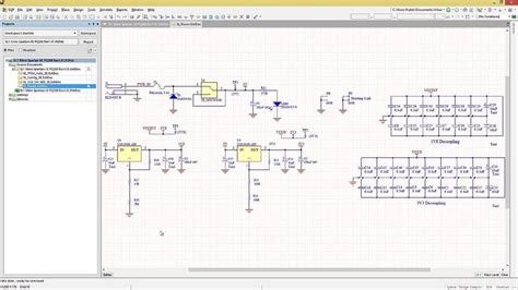
Creating Fabrication Drawings in Altium Designer
Setting Up the Drawing Environment
To create fabrication drawings in Altium Designer, start by setting up the drawing environment:
- Open your PCB design project in Altium Designer.
- Navigate to the “File” menu and select “New” > “Drawing”.
- Choose the appropriate drawing template (e.g., “Fabrication Drawing”) and click “OK”.
- Set the drawing properties, such as the sheet size and title block information.
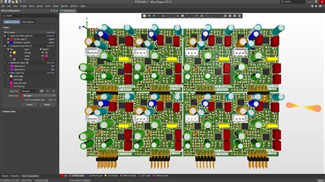
Adding Board Outline and Dimensions
To add the board outline and dimensions to your fabrication drawing:
- In the PCB editor, select the “View” menu and choose “Board Planning Mode”.
- Use the drawing tools to create the board outline and any necessary cutouts or slots.
- Add dimensions to the board outline using the “Dimension” tool in the drawing editor.
- Specify any tolerances or special requirements for the board dimensions.
Including Layer Stackup Information
To include the layer stackup information in your fabrication drawing:
- In the PCB editor, navigate to the “Design” menu and select “Layer Stack Manager”.
- Define the layer stackup, including the number of layers, material properties, and copper weights.
- Export the layer stackup information to a separate document or include it directly in the fabrication drawing.
Generating Drill Drawings
To generate drill drawings in Altium Designer:
- In the PCB editor, select the “File” menu and choose “Fabrication Outputs” > “Drill Drawing”.
- Configure the drill drawing settings, such as the hole sizes, symbols, and layer options.
- Generate the drill drawing and add it to your fabrication drawing set.
Exporting Copper Artwork and Solder Mask
To export the copper artwork and solder mask information:
- In the PCB editor, select the “File” menu and choose “Fabrication Outputs” > “Gerber Files”.
- Configure the Gerber file settings, such as the file format, aperture settings, and layer options.
- Generate the Gerber files for each copper layer and the solder mask layers.
- Include these files with your fabrication drawing set.
Adding Silkscreen and Fabrication Notes
To add silkscreen and fabrication notes to your drawing:
- In the drawing editor, use the text and graphics tools to add silkscreen elements, such as component outlines and labels.
- Include any necessary fabrication notes, such as special requirements for the manufacturing process or material specifications.
- Ensure that the silkscreen and fabrication notes are clear and easily readable.
Creating Assembly Drawings in Altium Designer
Setting Up the Drawing Environment
To create assembly drawings in Altium Designer, follow the same steps as for fabrication drawings:
- Open your PCB design project in Altium Designer.
- Navigate to the “File” menu and select “New” > “Drawing”.
- Choose the appropriate drawing template (e.g., “Assembly Drawing”) and click “OK”.
- Set the drawing properties, such as the sheet size and title block information.
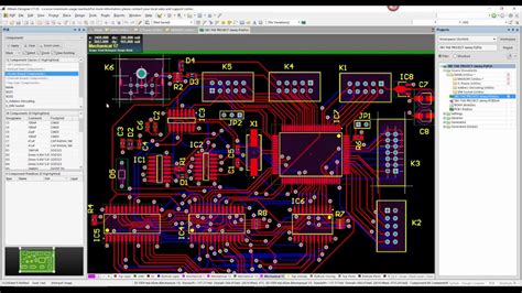
Placing Components and Reference Designators
To place components and reference designators in your assembly drawing:
- In the PCB editor, select the “View” menu and choose “Assembly Mode”.
- Use the “Place” tool to add component outlines and reference designators to the drawing.
- Ensure that the component placement matches the actual PCB layout.
- Include any necessary orientation indicators, such as pin 1 markers or polarity symbols.
Adding Assembly Notes and Instructions
To add assembly notes and instructions to your drawing:
- In the drawing editor, use the text and graphics tools to add assembly notes and instructions.
- Include any special requirements for the assembly process, such as hand soldering or specific torque values for fasteners.
- Ensure that the assembly notes are clear and easily understandable by the assembly team.
Generating the Bill of Materials (BOM)
To generate the BOM in Altium Designer:
- In the PCB editor, select the “Reports” menu and choose “Bill of Materials”.
- Configure the BOM settings, such as the included columns, sorting options, and file format.
- Generate the BOM and include it with your assembly drawing set.
- Ensure that the BOM contains all necessary component information, such as part numbers, quantities, and descriptions.
Collaborating with the Manufacturing Team
Effective Communication
Creating accurate and comprehensive fabrication and assembly drawings is only the first step in ensuring a successful PCB manufacturing process. Effective communication with the manufacturing team is equally important. To foster a collaborative relationship:
- Provide clear and concise documentation, including all necessary files and instructions.
- Be available to answer questions and provide clarifications as needed.
- Establish a feedback loop to address any issues or concerns that arise during the manufacturing process.
Design for Manufacturability (DFM)
To minimize manufacturing issues and ensure the best possible outcome, it is crucial to design your PCB with manufacturability in mind. This process, known as Design for Manufacturability (DFM), involves following best practices and guidelines that optimize the design for the manufacturing process. Some key DFM considerations include:
- Adhering to the manufacturer’s design rules and constraints.
- Choosing components that are readily available and compatible with the manufacturing process.
- Avoiding overly complex or dense designs that may be difficult to manufacture.
- Incorporating testability features to facilitate quality control and debugging.
By collaborating closely with the manufacturing team and following DFM principles, you can streamline the production process and minimize the risk of costly errors or delays.
Frequently Asked Questions (FAQ)
- What is the difference between fabrication and assembly drawings?
-
Fabrication drawings provide information for the PCB manufacturer to produce the bare board, while assembly drawings provide information for the assembly team to populate the board with components.
-
How do I ensure that my fabrication drawings are accurate?
-
To ensure accuracy, include all necessary information, such as board dimensions, layer stackup, and drill sizes. Use clear labeling and provide a comprehensive legend. Double-check all dimensions and specifications before finalizing the drawings.
-
What should I include in the BOM for my assembly drawings?
-
The BOM should include all components used in the assembly, along with their quantities, part numbers, and descriptions. Make sure to include any special handling or storage requirements for sensitive components.
-
How can I optimize my PCB design for manufacturability?
-
To optimize your design for manufacturability, follow the manufacturer’s design rules and constraints, choose readily available components, avoid overly complex designs, and incorporate testability features. Collaborate closely with the manufacturing team and be open to their feedback and suggestions.
-
What file formats should I use when exporting fabrication and assembly drawings?
- For fabrication drawings, use industry-standard file formats such as Gerber (RS-274X) for copper artwork and drill files (NC Drill or Excellon). For assembly drawings, use PDF or vector-based formats (e.g., DXF or SVG) for easy viewing and printing. Always consult with your manufacturer for their specific file format requirements.
Conclusion
Creating accurate and comprehensive fabrication and assembly drawings is essential for ensuring a smooth and successful PCB manufacturing process. By using Altium Designer’s powerful features and following best practices for drawing creation and communication with the manufacturing team, you can minimize the risk of errors and delays, and ultimately achieve a high-quality PCB that meets your design requirements.
Remember to include all necessary information in your drawings, such as board dimensions, layer stackup, component placement, and assembly instructions. Collaborate closely with the manufacturing team, follow DFM principles, and be open to feedback and suggestions to optimize your design for manufacturability.
By mastering the art of creating fabrication and assembly drawings in Altium Designer, you can streamline your PCB design workflow, improve communication with your manufacturing partners, and ultimately bring your electronic products to market faster and with higher quality.
Leave a Reply