Introduction to ESD Protection
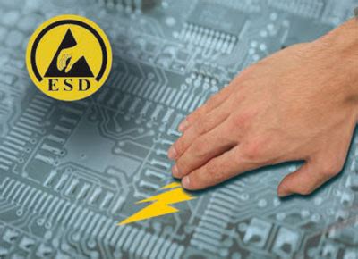
Electrostatic Discharge (ESD) is a common phenomenon that occurs when two objects with different electrical potentials come into contact or in close proximity to each other. In the context of electronic devices and printed circuit boards (PCBs), ESD can cause significant damage to sensitive components, leading to device failure or reduced performance. To mitigate the risks associated with ESD, it is crucial to implement effective ESD protection measures during the PCB design process.
In this beginner’s guide, we will explore the fundamentals of ESD protection circuit design for PCBs. We will cover the various types of ESD events, the importance of ESD protection, and the key components and techniques used in designing robust ESD protection circuits.
Understanding ESD Events
ESD events can be classified into three main categories based on their characteristics and the way they interact with electronic devices:
-
Human Body Model (HBM): This model represents the ESD event that occurs when a charged human body comes into contact with an electronic device. The HBM is characterized by a high-voltage, low-current discharge with a typical peak current of 1-10 A and a rise time of 2-10 ns.
-
Charged Device Model (CDM): The CDM represents the ESD event that occurs when a charged electronic device comes into contact with a grounded surface or another conductive object. CDM events are characterized by a high-current, low-voltage discharge with a peak current of 10-30 A and a rise time of less than 1 ns.
-
Machine Model (MM): The MM represents the ESD event that occurs when a charged machine or tool comes into contact with an electronic device. MM events are characterized by a high-voltage, high-current discharge with a peak current of 100-400 A and a rise time of 10-50 ns.
Understanding these ESD event models is essential for designing effective ESD protection circuits that can handle the specific characteristics of each type of discharge.
Importance of ESD Protection
ESD protection is crucial for ensuring the reliability and longevity of electronic devices and PCBs. Without proper ESD protection measures, sensitive components such as integrated circuits (ICs), transistors, and diodes can be damaged by the high-voltage and high-current transients generated during an ESD event.
The consequences of ESD damage can range from immediate device failure to latent defects that may manifest over time. Latent defects can be particularly problematic, as they may not be detected during initial testing and can lead to premature device failure in the field.
Implementing effective ESD protection circuits helps to:
- Prevent component damage and device failure
- Improve device reliability and longevity
- Reduce warranty claims and customer returns
- Comply with industry standards and regulations

Key Components of ESD Protection Circuits
ESD protection circuits typically consist of several key components that work together to divert the ESD energy away from sensitive components and provide a safe discharge path. The most common components used in ESD protection circuits include:
-
TVS Diodes: Transient Voltage Suppression (TVS) diodes are specialized Zener diodes designed to clamp the voltage across their terminals to a specific level when subjected to an ESD event. TVS diodes have a fast response time and can handle high peak currents, making them ideal for ESD protection applications.
-
Varistors: Varistors are voltage-dependent resistors that exhibit a non-linear resistance characteristic. When subjected to an ESD event, varistors rapidly decrease their resistance, allowing them to divert the ESD energy away from sensitive components.
-
Gas Discharge Tubes (GDTs): GDTs are two-terminal devices that consist of a sealed chamber filled with a special gas mixture. When the voltage across the GDT exceeds a certain threshold, the gas ionizes, creating a low-resistance path for the ESD energy to be discharged.
-
Polymer ESD Suppressors: Polymer ESD suppressors are relatively new devices that offer fast response times and low capacitance, making them suitable for high-speed applications. They consist of a polymer matrix filled with conductive particles that form a low-resistance path when subjected to an ESD event.
-
Series Resistors: Series resistors are often used in combination with other ESD protection components to limit the peak current during an ESD event. By placing a resistor in series with the signal path, the ESD energy is dissipated across the resistor, reducing the stress on the protected components.
ESD Protection Circuit Design Techniques
When designing ESD protection circuits for PCBs, several techniques can be employed to ensure optimal performance and protection:
-
Multilayer PCB Design: Using Multilayer PCBs allows for the creation of dedicated ESD protection layers, such as ground planes and power planes, which can help to distribute the ESD energy more evenly and reduce the risk of component damage.
-
Proper Grounding: Implementing a robust grounding scheme is essential for effective ESD protection. This includes using low-impedance ground connections, minimizing ground loops, and ensuring that all ESD protection components are properly connected to the ground plane.
-
Component Placement: Strategically placing ESD protection components close to the interfaces and connectors where ESD events are likely to occur can help to minimize the PCB Trace length and reduce the inductance, improving the overall ESD protection performance.
-
Signal Integrity Considerations: When designing ESD protection circuits, it is important to consider the impact on signal integrity. ESD protection components can introduce capacitance and inductance to the signal path, which can degrade high-speed signals. Careful component selection and placement can help to minimize these effects.
-
Simulation and Testing: Conducting ESD simulations and testing during the design process can help to validate the effectiveness of the ESD protection circuit and identify potential weaknesses. Industry-standard ESD testing methods, such as the Human Body Model (HBM) and the Charged Device Model (CDM), should be used to ensure compliance with relevant standards.
ESD Protection Standards and Regulations
Several industry standards and regulations govern the ESD protection requirements for electronic devices and PCBs. Some of the most common standards include:
-
IEC 61000-4-2: This international standard defines the ESD immunity test methods and levels for electronic equipment. It covers both contact discharge and air discharge test methods and specifies the voltage levels and waveforms to be used during testing.
-
ANSI/ESDA/JEDEC JS-001: This joint standard by the American National Standards Institute (ANSI), the ESD Association (ESDA), and the JEDEC Solid State Technology Association defines the HBM ESD test method and classification levels for electronic components.
-
ANSI/ESDA/JEDEC JS-002: This joint standard defines the CDM ESD test method and classification levels for electronic components.
-
MIL-STD-883, Method 3015: This military standard defines the ESD test methods and levels for electronic components used in military and aerospace applications.
Complying with these standards and regulations ensures that electronic devices and PCBs are designed to withstand the specified ESD stress levels and maintain reliable operation in the intended environment.
FAQs
-
What is the difference between TVS diodes and varistors?
TVS diodes and varistors are both used for ESD protection, but they have some key differences. TVS diodes are specifically designed for fast response times and high peak current handling, while varistors offer a more gradual clamping action and are better suited for lower-frequency transients. TVS diodes also have a lower capacitance compared to varistors, making them more suitable for high-speed applications. -
Can I use a single ESD protection component for all interfaces on my PCB?
While it is possible to use a single ESD protection component for multiple interfaces, it is generally recommended to use dedicated protection components for each interface. This ensures optimal protection performance and minimizes the risk of ESD energy propagating between interfaces. Additionally, different interfaces may have different ESD protection requirements, such as voltage levels and capacitance limits, which should be considered when selecting protection components. -
How do I select the appropriate voltage rating for my ESD protection components?
When selecting the voltage rating for ESD protection components, consider the maximum operating voltage of the protected interface and the expected ESD stress levels. The voltage rating of the protection component should be higher than the maximum operating voltage to avoid inadvertent clamping during normal operation. However, it should be low enough to effectively clamp the voltage during an ESD event. Consulting the relevant ESD protection standards and component datasheets can help in selecting the appropriate voltage rating. -
What is the role of series resistors in ESD protection circuits?
Series resistors are often used in combination with other ESD protection components to limit the peak current during an ESD event. By placing a resistor in series with the signal path, the ESD energy is dissipated across the resistor, reducing the stress on the protected components. Series resistors also help to minimize the capacitive loading on high-speed signals introduced by the ESD protection components. The value of the series resistor should be carefully selected to balance ESD protection effectiveness and signal integrity. -
How do I test the effectiveness of my ESD protection circuit?
To test the effectiveness of an ESD protection circuit, industry-standard ESD testing methods should be used. The most common methods include the Human Body Model (HBM) and the Charged Device Model (CDM). These tests involve subjecting the PCB or device to specified ESD stress levels and waveforms while monitoring for any signs of damage or degradation. ESD testing can be performed in-house using specialized equipment or by engaging the services of a certified ESD testing laboratory.
Conclusion
Designing effective ESD protection circuits is crucial for ensuring the reliability and longevity of electronic devices and PCBs. By understanding the different types of ESD events, the key components used in ESD protection, and the various design techniques and standards, engineers can create robust ESD protection solutions that safeguard sensitive components from the damaging effects of electrostatic discharge.
When designing ESD protection circuits, it is essential to consider factors such as component selection, placement, grounding, and signal integrity. Conducting simulations and testing during the design process can help to validate the effectiveness of the protection circuit and ensure compliance with relevant industry standards.
By following the guidelines and best practices outlined in this beginner’s guide, engineers can confidently design ESD protection circuits that meet the specific requirements of their applications and provide reliable protection against the ever-present threat of ESD.
Key Takeaways
- ESD protection is essential for preventing component damage and ensuring device reliability
- Different types of ESD events, such as HBM, CDM, and MM, have specific characteristics that must be considered in protection circuit design
- Key components used in ESD protection include TVS diodes, varistors, GDTs, polymer suppressors, and series resistors
- Proper PCB design techniques, such as multilayer design, grounding, and component placement, are crucial for effective ESD protection
- Industry standards and regulations, such as IEC 61000-4-2 and ANSI/ESDA/JEDEC JS-001, provide guidance on ESD protection requirements and testing methods
- Simulation and testing are essential for validating the effectiveness of ESD protection circuits and ensuring compliance with relevant standards
By understanding and applying these key concepts, engineers can create robust and reliable ESD protection solutions for their PCB designs, ensuring the long-term performance and success of their electronic devices.
Leave a Reply