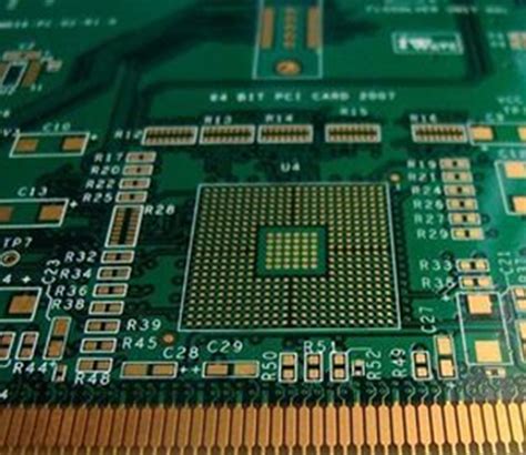
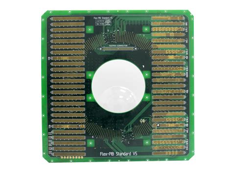
What are Multilayer PCBs?
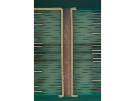
Multilayer PCBs are printed circuit boards that consist of three or more conductive copper layers laminated together with insulating material between each layer. These layers are interconnected using plated through-holes (vias) to create a complex circuit. Multilayer PCBs offer several advantages over single or double-layer boards, including:
- Increased circuit density and functionality
- Reduced board size and weight
- Improved signal integrity and electromagnetic interference (EMI) shielding
- Enhanced thermal management and power distribution
Types of Multilayer PCBs
There are several types of multilayer PCBs, each designed for specific applications and manufacturing processes:
| Type | Description |
|---|---|
| Standard Multilayer | The most common type, with alternating layers of copper and insulating material. |
| High Density Interconnect (HDI) | Uses microvias and thin dielectric layers for high-density component placement. |
| Rigid-Flex | Combines rigid and flexible layers for applications requiring both stability and flexibility. |
| Buried/Blind Vias | Uses vias that do not extend through the entire board thickness, allowing for more complex routing. |
Designing Multilayer PCBs
Layer Stack-up
The layer stack-up is a critical aspect of multilayer PCB design. It determines the number, order, and thickness of the conductive and insulating layers. A typical 4-layer stack-up might look like this:
| Layer | Material | Thickness (mm) |
|---|---|---|
| Top Copper | Copper | 0.035 |
| Dielectric 1 | FR-4 | 0.2 |
| Inner Copper 1 | Copper | 0.035 |
| Core | FR-4 | 0.4 |
| Inner Copper 2 | Copper | 0.035 |
| Dielectric 2 | FR-4 | 0.2 |
| Bottom Copper | Copper | 0.035 |
The stack-up should be carefully designed to ensure proper signal integrity, impedance control, and manufacturability.
Signal Integrity
Signal integrity is a critical concern in multilayer PCB design. As signals travel through the board, they can be affected by various factors, including:
- Crosstalk between adjacent traces
- Reflections due to impedance mismatches
- EMI from external sources or other parts of the circuit
To mitigate these issues, designers can use techniques such as:
- Proper trace routing and spacing
- Controlled impedance traces
- Ground planes and power planes for shielding and low-impedance power distribution
- Decoupling capacitors to reduce power supply noise
Thermal Management
Multilayer PCBs can generate significant heat, especially in high-power applications. Proper thermal management is essential to ensure reliable operation and prevent component failure. Some strategies for thermal management include:
- Using thicker copper layers for power and ground planes
- Incorporating thermal vias to conduct heat away from components
- Using heat sinks and other external cooling solutions
- Selecting components with appropriate power ratings and thermal characteristics

Manufacturing Multilayer PCBs
Fabrication Process
The fabrication process for multilayer PCBs involves several steps:
- Inner layer processing: The inner copper layers are patterned and etched.
- Lamination: The inner layers are laminated together with insulating material.
- Drilling: Through-holes and vias are drilled through the laminated board.
- Plating: The through-holes and vias are plated with copper to create electrical connections between layers.
- Outer layer processing: The outer copper layers are patterned and etched.
- Solder mask and silkscreen: A protective solder mask and silkscreen legends are applied.
- Surface finish: A surface finish, such as HASL or ENIG, is applied to protect the copper and facilitate soldering.
Design for Manufacturability (DFM)
To ensure successful manufacturing, multilayer PCBs must be designed with manufacturability in mind. Some key DFM considerations include:
- Adhering to minimum trace width and spacing requirements
- Avoiding acute angles and sharp corners in traces
- Providing sufficient clearance around through-holes and vias
- Specifying appropriate tolerances for hole sizes and layer registration
- Selecting materials and finishes that are compatible with the intended manufacturing process

Applications of Multilayer PCBs
Multilayer PCBs are used in a wide range of applications, including:
- Consumer electronics: Smartphones, tablets, laptops, and wearables
- Automotive: Engine control units, infotainment systems, and advanced driver assistance systems (ADAS)
- Medical devices: Imaging equipment, patient monitors, and implantable devices
- Industrial automation: Programmable logic controllers (PLCs), sensors, and motor drives
- Aerospace and defense: Avionics, radar systems, and satellite communications

Frequently Asked Questions (FAQ)
-
Q: What is the minimum number of layers required for a multilayer PCB?
A: A multilayer PCB must have at least three conductive layers, although most designs use four or more layers. -
Q: Can multilayer PCBs be flexible?
A: Yes, rigid-flex PCBs combine rigid and flexible layers to create boards that can bend or fold as needed. -
Q: What materials are used for the insulating layers in multilayer PCBs?
A: The most common insulating material is FR-4, a glass-reinforced epoxy laminate. Other materials, such as polyimide or PTFE, may be used for high-frequency or high-temperature applications. -
Q: How small can the vias be in a multilayer PCB?
A: The minimum via size depends on the manufacturing process and the number of layers. Modern HDI processes can create microvias as small as 0.1 mm in diameter. -
Q: What is the maximum number of layers that can be used in a multilayer PCB?
A: While there is no theoretical limit, most commercial multilayer PCBs have between 4 and 12 layers. Some specialized applications may use boards with 20 or more layers, but these are rare and expensive to manufacture.
Conclusion
Multilayer PCBs are an essential technology for modern electronics, enabling the creation of complex, high-density circuits in a compact and reliable package. By understanding the design, manufacturing, and application considerations for multilayer PCBs, engineers can create innovative products that push the boundaries of performance and functionality. As electronic systems continue to evolve, multilayer PCBs will remain a critical component of the design and manufacturing process.

Leave a Reply