Introduction to PCB Manufacturing
Printed circuit board (PCB) manufacturing is the process of creating circuit boards that electrically connect electronic components using conductive tracks, pads and other features etched from one or more sheet layers of copper laminated onto and/or between sheet layers of a non-conductive substrate. PCBs are used in virtually all electronic products including computers, smartphones, appliances, medical equipment and aerospace systems.
The PCB manufacturing process involves several key steps:
1. Design: Creating the schematic and layout of the PCB
2. Fabrication: Printing and etching the copper layers and drilling holes
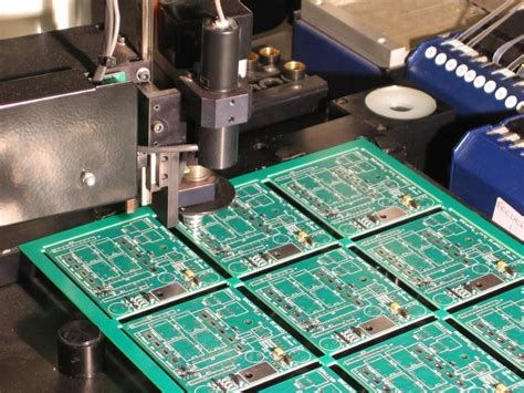
3. Assembly: Soldering components onto the fabricated board
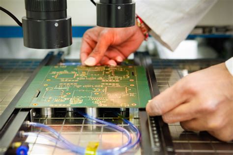
4. Testing: Verifying the assembled board functions properly
5. Finishing: Applying protective coatings and treatments
Each step requires careful planning, execution and quality control to ensure the final PCB performs reliably in the end application. Errors or defects introduced at any stage can compromise the entire board. That’s why it’s critical to start with an accurate and comprehensive bill of materials.
The Importance of a Complete Bill of Materials
The bill of materials (BOM) is the complete list of parts and materials required to manufacture the PCB, including both fabrication and assembly. It should specify:
- The type, value, footprint, and quantity of each component
- The manufacturer and manufacturer part number (MPN) for each component
- The type, thickness, and copper weight of the PCB base material
- The surface finish for exposed copper (e.g. HASL, ENIG, OSP)
- Any special requirements for solder mask, silkscreen, gold fingers, etc.
An accurate and complete BOM is essential for several reasons:
- It ensures the correct parts are ordered and used in production
- It allows the fabricator and assembler to properly quote the job
- It provides a clear blueprint for the manufacturing process
- It serves as a reference for testing, troubleshooting and repairs
Without a proper BOM, there is a high risk of errors such as using the wrong components, ordering insufficient quantities, or omitting required parts altogether. These mistakes can be costly in terms of scrapped materials, wasted labor, delayed shipments and field failures.
Example BOM
Here is an example of what a typical BOM might include:
| Designator | Qty | Value | Description | Footprint | MPN |
|---|---|---|---|---|---|
| C1-C10 | 10 | 0.1uF | Capacitor | 0805 | CL21B104KBCNNNC |
| R1-R5 | 5 | 10K | Resistor | 0603 | RC0603FR-0710KL |
| U1 | 1 | ATMEGA328P-AU | MCU | TQFP-32 | ATMEGA328P-AU |
| PCB | 1 | FR4 | 1.6mm 1oz Cu | – | – |
| Finish | – | HASL | Lead-Free HASL | – | – |
Other Suggestions for Error Free PCB Manufacturing
In addition to starting with a complete and accurate BOM, there are several other best practices that can help ensure a smooth and successful PCB manufacturing process:
Use Standard Components and Footprints
Wherever possible, select components that are readily available and use standard footprints. This will make it easier for the assembler to source the parts and reduce the risk of errors in the pick-and-place process. If custom or unusual parts are required, be sure to provide detailed specifications and work closely with the supplier to ensure compatibility.
Follow Fabrication Design Rules
Each PCB fabricator has its own set of design rules and guidelines based on their equipment and processes. These cover aspects such as minimum trace width and spacing, drill hole sizes, annular rings, etc. By following the fabricator’s design rules from the start, you can avoid issues such as low yields or non-manufacturability.
Some common PCB design rules include:
- Minimum trace width: 0.006″ (0.15mm)
- Minimum trace spacing: 0.006″ (0.15mm)
- Minimum drill hole size: 0.020″ (0.50mm)
- Minimum annular ring: 0.005″ (0.13mm)
Perform Design Rule Checks
Most PCB design software includes automated design rule checking (DRC) tools that can detect and flag violations of the fabricator’s design rules. Running DRC early and often during the layout process can catch errors before they become embedded in the design. Be sure to also double-check the final Gerber files before sending them to the fabricator.
Communicate Clearly with Fabricator and Assembler
Clear and continuous communication with the fabricator and assembler is essential for avoiding misunderstandings and mistakes. Provide them with complete and accurate documentation, including the BOM, Gerber files, assembly drawings, and any special instructions. Be available to answer questions and clarify requirements throughout the process.
Allow Adequate Time for Production
Rushing a PCB manufacturing job is a recipe for errors and defects. Be sure to allow adequate time in the schedule for each stage of production, plus additional time for unexpected delays. Work with the fabricator and assembler to set realistic lead times based on the complexity of the design and the current production workload.

Conclusion
In summary, a complete and accurate bill of materials is the foundation for error-free PCB manufacturing. By also following design rules, performing DRC, communicating clearly, and allowing adequate production time, you can further reduce the risk of mistakes and ensure a high-quality end product.
FAQ
What happens if a part on the BOM becomes obsolete?
If a part on the BOM becomes obsolete or unavailable, it will need to be replaced with a suitable substitute. This may require updating the schematic, layout and documentation to reflect the change. The earlier in the process that the obsolescence is identified, the easier it will be to make the necessary changes.
Can I use different fabricators and assemblers for the same design?
In general, it is best to use the same fabricator and assembler for a given PCB design in order to ensure consistency and compatibility. If different suppliers must be used, be sure that they are working from the same BOM, Gerber files and specifications. Pay close attention to any differences in their capabilities or processes that could affect the end result.
What is the difference between a parts list and a BOM?
A parts list is simply a list of the components used in a design, typically organized by value or type. A BOM, on the other hand, is a more comprehensive document that also specifies the quantity, package type, manufacturer part number, and other details needed to actually purchase and assemble the components onto the PCB.
How do I create a BOM?
Most PCB design software can automatically generate a BOM from the schematic and layout data. However, it is important to carefully review and edit the generated BOM to ensure accuracy and completeness. This may involve adding additional details such as manufacturer part numbers, specifying alternate parts, or including non-electronic items such as mounting hardware or cables.
What should I do if I find an error on the PCB after manufacturing?
If an error is discovered on the PCB after manufacturing, the first step is to assess the severity and scope of the problem. Small errors may be repairable by rework, while larger errors may require scrapping the affected boards and starting over. In either case, it is important to fully investigate the root cause of the error and take corrective action to prevent it from recurring in the future. This may involve updating the BOM, design files, or manufacturing processes.
Leave a Reply