Introduction to Hierarchical Schematics
In the world of electronic circuit design, creating and managing complex schematics can be a daunting task. As circuits grow in size and complexity, traditional flat schematic representations become increasingly difficult to navigate, understand, and maintain. This is where the concept of hierarchical schematics comes into play, revolutionizing the way designers approach circuit design.
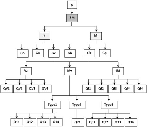
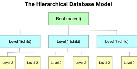
A hierarchical schematic is a powerful tool that allows designers to break down a complex circuit into smaller, more manageable sub-circuits or modules. By organizing the schematic in a hierarchical manner, designers can create a clear and logical structure that enhances readability, promotes reusability, and simplifies the overall design process.
Benefits of Using Hierarchical Schematics
-
Improved Readability: By breaking down a complex circuit into smaller, self-contained modules, hierarchical schematics make it easier for designers to understand the overall functionality and interconnections of the circuit.
-
Enhanced Reusability: Hierarchical schematics enable the creation of reusable sub-circuits or modules that can be easily integrated into multiple designs, saving time and effort.
-
Simplified Collaboration: With a hierarchical structure, multiple designers can work on different parts of the circuit simultaneously, facilitating efficient collaboration and parallel development.
-
Reduced Errors: By organizing the schematic into logical modules, designers can minimize the risk of errors and inconsistencies, as each module can be individually tested and verified.
Creating a Hierarchical Schematic
Step 1: Identify Functional Blocks
The first step in creating a hierarchical schematic is to identify the functional blocks or modules within the circuit. Each block should represent a specific functionality or a group of related components. For example, in a digital clock circuit, you might have separate blocks for the power supply, time-keeping logic, display driver, and user interface.
Step 2: Define Interfaces
Once the functional blocks are identified, the next step is to define the interfaces between them. Interfaces specify the inputs, outputs, and any control signals that connect the blocks together. Clear and well-defined interfaces ensure proper communication and data flow between the modules.
Step 3: Create Sub-Schematics
For each functional block, create a separate sub-schematic that contains the detailed circuitry for that specific module. The sub-schematic should have its own set of input and output ports that match the defined interfaces. This allows for a clean separation of concerns and makes the overall schematic more modular and manageable.
Step 4: Assign Hierarchical Symbols
To represent the sub-schematics in the top-level schematic, assign hierarchical symbols to each functional block. These symbols act as placeholders for the detailed sub-schematics and provide a high-level view of the circuit’s structure. The hierarchical symbols should clearly indicate the inputs, outputs, and any relevant information about the module.
Step 5: Connect the Hierarchical Symbols
In the top-level schematic, connect the hierarchical symbols according to the defined interfaces. Use appropriate signal names and busses to establish the connections between the modules. This top-level schematic serves as a roadmap for the overall circuit, showing how the different functional blocks interact with each other.
Step 6: Document and Annotate
To ensure clarity and maintainability, it is crucial to document and annotate the hierarchical schematic. Provide meaningful names for the functional blocks, signals, and busses. Include comments and notes to explain the purpose and functionality of each module. Well-documented schematics make it easier for other designers to understand and work with the circuit.
Best Practices for Hierarchical Schematic Design
-
Keep Modules Focused: Each functional block should have a clear and specific purpose. Avoid overloading a module with too many responsibilities, as it can reduce readability and maintainability.
-
Use Consistent Naming Conventions: Establish and follow consistent naming conventions for modules, signals, and components throughout the hierarchical schematic. This helps in avoiding confusion and ensures a cohesive design.
-
Minimize Interconnections: Strive to minimize the number of interconnections between modules. A well-designed hierarchical schematic should have clean and concise interfaces, reducing the complexity of the overall circuit.
-
Reuse Common Modules: Identify and create reusable modules that can be used across multiple projects or designs. This saves time, reduces duplication of effort, and promotes standardization.
-
Regularly Review and Refactor: As the circuit evolves, regularly review and refactor the hierarchical schematic. Look for opportunities to optimize the design, improve modularity, and address any inconsistencies or redundancies.

Hierarchical Schematic Tools and Software
To effectively create and manage hierarchical schematics, designers rely on specialized tools and software. These tools provide a range of features and capabilities that streamline the design process and enhance productivity. Some popular hierarchical schematic tools include:
| Tool | Description | Key Features |
|---|---|---|
| Altium Designer | A comprehensive PCB design software with hierarchical schematic capabilities. | – Hierarchical design support – Real-time synchronization between schematic and PCB – Extensive library management |
| OrCAD Capture | A widely used schematic capture tool that supports hierarchical design. | – Hierarchical block-based design – Automated annotation and back-annotation – Integration with simulation and PCB layout tools |
| KiCad EDA | A free and open-source EDA software suite with hierarchical schematic functionality. | – Hierarchical sheet-based design – Cross-probing between schematic and PCB – Integrated library management |
| Eagle | A popular PCB design software that offers hierarchical schematic capabilities. | – Hierarchical sheet support – Automatic forward and back-annotation – Extensive component libraries |
These tools provide a user-friendly interface for creating and managing hierarchical schematics, with features such as drag-and-drop placement, automatic annotation, and cross-probing between schematic and PCB views.

Frequently Asked Questions (FAQ)
-
Q: What is the main advantage of using hierarchical schematics over flat schematics?
A: The main advantage of hierarchical schematics is the ability to break down a complex circuit into smaller, more manageable sub-circuits or modules. This improves readability, promotes reusability, and simplifies the overall design process. -
Q: How do I decide when to split a circuit into multiple hierarchical levels?
A: The decision to split a circuit into hierarchical levels depends on the complexity and functionality of the circuit. If a particular section of the circuit has a distinct function or can be reused in other designs, it is a good candidate for a separate hierarchical level. -
Q: Can hierarchical schematics be used for both analog and digital circuits?
A: Yes, hierarchical schematics can be used for both analog and digital circuits. The principles of breaking down a circuit into functional blocks and defining interfaces apply to both domains. -
Q: How do I ensure consistency and compatibility between different hierarchical levels?
A: To ensure consistency and compatibility, it is important to establish and follow clear naming conventions, define well-structured interfaces between modules, and regularly review and refactor the hierarchical schematic as the design evolves. -
Q: Are there any limitations or challenges associated with hierarchical schematic design?
A: One potential challenge with hierarchical schematic design is the increased complexity in managing and tracking changes across multiple levels. It is important to have robust version control and documentation practices in place to mitigate this challenge.
Conclusion
Hierarchical schematics provide a powerful and efficient approach to circuit design, enabling designers to create complex systems with improved readability, reusability, and maintainability. By breaking down a circuit into smaller, self-contained modules and defining clear interfaces between them, hierarchical schematics streamline the design process and facilitate collaboration among team members.
To successfully implement hierarchical schematics, designers should follow best practices such as keeping modules focused, using consistent naming conventions, minimizing interconnections, reusing common modules, and regularly reviewing and refactoring the design. Specialized tools and software, such as Altium Designer, OrCAD Capture, KiCad EDA, and Eagle, offer robust features and capabilities to support hierarchical schematic design.
By embracing the hierarchical schematic approach and leveraging the available tools and best practices, designers can unlock new levels of efficiency, clarity, and innovation in their circuit designs. Whether working on analog or digital circuits, hierarchical schematics provide a solid foundation for creating complex and reliable electronic systems.
Leave a Reply