Why PCB Design Reviews Are Essential
PCB design reviews are crucial for several reasons:
-
Identifying design issues early: By catching problems during the design phase, you can avoid costly manufacturing delays and redesigns later in the development cycle.
-
Ensuring manufacturability: Design reviews help confirm that your PCB can be manufactured efficiently and cost-effectively, considering factors such as component placement, routing, and design rules compliance.
-
Verifying functionality: Reviews allow you to double-check that your PCB design meets all functional requirements and will perform as expected once manufactured.
-
Facilitating collaboration: Design reviews provide an opportunity for team members and stakeholders to provide input and feedback, fostering a collaborative environment and ensuring all requirements are met.
When to Conduct PCB Design Reviews
PCB design reviews should be conducted at various stages throughout the design process:
Schematic Review
The first review should occur after creating the schematic. This review focuses on:
- Correct component selection
- Proper connections between components
- Power supply and grounding scheme
- Signal integrity considerations
Placement Review
After component placement, review the layout to ensure:
- Optimal component positioning for manufacturability and functionality
- Proper placement of connectors, mounting holes, and other mechanical features
- Adequate spacing between components for assembly and heat dissipation
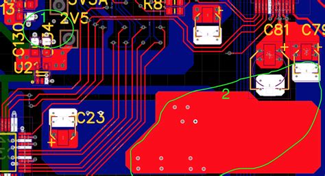
Routing Review
Once routing is complete, review the PCB layout to check:
- Trace widths and spacing meet design rules
- High-speed signals are routed correctly
- Proper use of vias and layer transitions
- Sufficient ground and power plane coverage
Final Design Review
Before sending the design for manufacturing, conduct a final comprehensive review to verify:
- All previous review feedback has been addressed
- Design meets all functional and performance requirements
- Manufacturing files are complete and accurate
Best Practices for Conducting PCB Design Reviews
To make your PCB design reviews as effective as possible, follow these best practices:
1. Use Checklists
Create standardized checklists for each review stage to ensure consistency and thoroughness. Checklists should cover all critical aspects of the design, such as:
- Component selection and placement
- Schematic and layout design rules
- Signal integrity and power integrity
- Manufacturability and assembly considerations
2. Involve the Right Stakeholders
Include all relevant stakeholders in the review process, such as:
- PCB designers
- Electrical engineers
- Mechanical engineers
- Manufacturing and assembly experts
- Quality assurance professionals
- Project managers
Involving a diverse team helps catch a wider range of issues and ensures all perspectives are considered.
3. Use Design Review Tools
Leverage PCB design review tools to streamline the process and make it more efficient. Some popular tools include:
- Design rule checking (DRC) software
- Electrical rule checking (ERC) tools
- Signal and power integrity simulation tools
- Collaborative design review platforms
These tools automate many aspects of the review process, saving time and reducing the risk of human error.
4. Document and Track Issues
Maintain a centralized system for documenting and tracking design review issues. This can be as simple as a spreadsheet or a more sophisticated issue-tracking tool. For each issue, record:
- Description of the problem
- Severity level (e.g., critical, major, minor)
- Person responsible for resolving the issue
- Target resolution date
- Status (e.g., open, in progress, resolved)
Regularly update the issue tracker and communicate progress to the team to ensure all issues are addressed in a timely manner.
5. Foster Open Communication
Encourage open, honest communication during design reviews. Create an environment where team members feel comfortable raising concerns and offering suggestions for improvement. Avoid assigning blame and instead focus on finding solutions collaboratively.

Common PCB Design Review Issues and How to Address Them
During PCB design reviews, several common issues may arise. Here are some examples and how to address them:
Issue 1: Incorrect Component Selection
Problem: The wrong component is selected for a particular function, leading to performance issues or incompatibility with other components.
Solution: Double-check component datasheets and consult with the electrical engineering team to ensure the correct components are selected. Consider factors such as voltage and current ratings, package size, and temperature range.
Issue 2: Inadequate Clearance Between Components
Problem: Components are placed too close together, making assembly difficult or increasing the risk of short circuits.
Solution: Adhere to the manufacturer’s recommended clearance guidelines and consider the assembly process when placing components. Use PCB layout tools to automatically check for clearance violations.
Issue 3: Incorrect Trace Widths and Spacing
Problem: Trace widths and spacing do not meet the design rules, leading to manufacturing issues or signal integrity problems.
Solution: Use PCB design software to define and check design rules automatically. Consult with the manufacturing team to ensure trace widths and spacing are appropriate for the chosen fabrication process.
Issue 4: Signal Integrity Issues
Problem: High-speed signals are not routed properly, resulting in crosstalk, reflections, or other signal integrity problems.
Solution: Follow best practices for high-speed PCB design, such as minimizing trace lengths, using appropriate termination techniques, and properly routing differential pairs. Use signal integrity simulation tools to analyze and optimize the design.
Issue 5: Insufficient Power and Ground Plane Coverage
Problem: The PCB lacks adequate power and ground plane coverage, leading to voltage drop, noise, and other power integrity issues.
Solution: Ensure power and ground planes are properly sized and positioned to provide low-impedance paths for current flow. Use power integrity simulation tools to analyze the design and make necessary adjustments.
PCB Review FAQ
-
Q: How long does a typical PCB design review take?
A: The duration of a PCB design review can vary depending on the complexity of the design and the number of issues found. Generally, plan for at least a few hours to a full day for each review stage. -
Q: Who should be involved in PCB design reviews?
A: PCB design reviews should involve all relevant stakeholders, including PCB designers, electrical engineers, mechanical engineers, manufacturing and assembly experts, quality assurance professionals, and project managers. -
Q: What tools are used for PCB design reviews?
A: Common tools used for PCB design reviews include design rule checking (DRC) software, electrical rule checking (ERC) tools, signal and power integrity simulation tools, and collaborative design review platforms. -
Q: How often should PCB design reviews be conducted?
A: PCB design reviews should be conducted at key stages throughout the design process, including schematic review, placement review, routing review, and final design review before manufacturing. -
Q: What should I do if issues are found during a PCB design review?
A: Document the issues in a centralized issue tracker, assign responsibility for resolving each issue, and set target resolution dates. Regularly update the issue tracker and communicate progress to the team to ensure all issues are addressed before moving forward with manufacturing.
| Review Stage | Focus Areas | Tools |
|---|---|---|
| Schematic Review | – Component selection – Connections – Power and grounding – Signal integrity |
– ERC tools – Simulation tools |
| Placement Review | – Component positioning – Mechanical features – Spacing for assembly and heat dissipation |
– PCB layout tools – 3D modeling tools |
| Routing Review | – Trace widths and spacing – High-speed signal routing – Vias and layer transitions – Ground and power plane coverage |
– DRC tools – Signal integrity simulation tools – Power integrity simulation tools |
| Final Design Review | – All previous feedback addressed – Functional and performance requirements met – Manufacturing files complete and accurate |
– Collaborative design review platforms – Issue tracking tools |
By following the best practices outlined in this guide and conducting thorough PCB design reviews at each stage of the development process, you can create high-quality, reliable PCBs that meet all functional and performance requirements. Remember to involve the right stakeholders, use appropriate tools, and foster open communication to make your PCB design reviews as effective and efficient as possible.
Leave a Reply