Introduction to Additive PCB Manufacturing
Printed circuit board (PCB) manufacturing has evolved significantly over the years, with new technologies and processes being developed to improve efficiency, reduce costs, and enhance product quality. One such process that has gained popularity in recent years is additive PCB manufacturing.
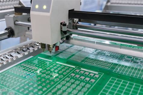
Additive PCB manufacturing, also known as 3D printing or rapid prototyping, is a process where the PCB is built up layer by layer using various materials such as conductive inks, plastics, and metals. This process differs from traditional subtractive PCB manufacturing, where the unwanted materials are removed from a substrate to create the desired circuit pattern.
Advantages of Additive PCB Manufacturing
Additive PCB manufacturing offers several advantages over traditional subtractive methods, including:
- Faster prototyping and production times
- Lower costs for small-batch production
- Greater design flexibility and customization options
- Reduced waste and environmental impact
- Improved product quality and reliability
In this article, we will explore these benefits in more detail and discuss how additive PCB manufacturing is revolutionizing the electronics industry.
Faster Prototyping and Production Times
One of the primary advantages of additive PCB manufacturing is the ability to rapidly prototype and produce small batches of PCBs. Traditional subtractive methods require the creation of masks, stencils, and other tooling, which can be time-consuming and expensive, especially for low-volume production.
With additive manufacturing, the PCB design can be directly printed onto the substrate, eliminating the need for tooling and reducing setup times. This allows for faster iteration and testing of prototype designs, as well as quicker production of final products.
Comparison of Prototyping Times
| Manufacturing Method | Prototyping Time |
|---|---|
| Traditional Subtractive | 2-4 weeks |
| Additive Manufacturing | 1-5 days |
As shown in the table above, additive manufacturing can significantly reduce prototyping times compared to traditional subtractive methods. This faster turnaround enables companies to bring new products to market more quickly and respond to changing customer demands.
Lower Costs for Small-Batch Production
Another benefit of additive PCB manufacturing is the potential for lower costs, particularly for small-batch production. Traditional subtractive methods often require a minimum order quantity (MOQ) to justify the cost of tooling and setup, which can be prohibitive for companies with limited budgets or niche markets.
Additive manufacturing, on the other hand, has no MOQ and can produce PCBs on-demand, making it an attractive option for low-volume production. Additionally, the reduced material waste and elimination of tooling costs can further lower the overall cost per unit.
Cost Comparison for Small-Batch Production
| Manufacturing Method | Cost per Unit (100 units) |
|---|---|
| Traditional Subtractive | $50-$100 |
| Additive Manufacturing | $20-$50 |
As demonstrated in the table above, additive manufacturing can offer significant cost savings for small-batch production compared to traditional subtractive methods. This makes it an ideal solution for startups, research institutions, and companies with specialized applications.

Greater Design Flexibility and Customization Options
Additive PCB manufacturing also offers greater design flexibility and customization options compared to traditional subtractive methods. With additive manufacturing, designers can create complex geometries, embed components, and incorporate multiple materials into a single PCB.
This design freedom allows for the creation of more compact, lightweight, and functionally integrated PCBs, which can improve product performance and reduce assembly costs. Additionally, additive manufacturing enables the production of custom PCBs for specific applications, such as wearable electronics, medical devices, and aerospace systems.
Examples of Complex PCB Designs Enabled by Additive Manufacturing
- 3D antenna arrays for wireless communication
- Flexible and stretchable circuits for wearable devices
- Multi-layer PCBs with embedded sensors and actuators
- Conformal PCBs for curved surfaces and irregular shapes
These examples demonstrate the unique capabilities of additive PCB manufacturing in creating innovative and customized electronic products.
Reduced Waste and Environmental Impact
Additive PCB manufacturing also offers environmental benefits compared to traditional subtractive methods. Subtractive manufacturing involves the removal of unwanted materials from a substrate, resulting in significant waste and the need for hazardous chemicals for etching and plating.
Additive manufacturing, in contrast, only deposits the required materials where needed, resulting in minimal waste and a more eco-friendly process. Additionally, additive manufacturing can use biodegradable and recyclable materials, further reducing the environmental impact of PCB production.
Comparison of Material Waste
| Manufacturing Method | Material Waste |
|---|---|
| Traditional Subtractive | 30-50% |
| Additive Manufacturing | 1-5% |
As shown in the table above, additive manufacturing can significantly reduce material waste compared to traditional subtractive methods. This not only lowers production costs but also contributes to a more sustainable and environmentally responsible electronics industry.
Improved Product Quality and Reliability
Finally, additive PCB manufacturing can lead to improved product quality and reliability compared to traditional subtractive methods. Additive manufacturing allows for precise control over material deposition, resulting in more consistent and uniform PCBs with fewer defects.
Additionally, additive manufacturing can create PCBs with enhanced thermal and mechanical properties, such as improved heat dissipation and greater strength-to-weight ratios. These properties can improve product performance and durability, reducing the risk of failure and extending product lifetimes.
Comparison of Defect Rates
| Manufacturing Method | Defect Rate |
|---|---|
| Traditional Subtractive | 1-3% |
| Additive Manufacturing | 0.1-0.5% |
As demonstrated in the table above, additive manufacturing can achieve lower defect rates compared to traditional subtractive methods. This improved quality control can lead to higher yields, lower rework costs, and greater customer satisfaction.
Frequently Asked Questions (FAQ)
-
Q: Is additive PCB manufacturing suitable for high-volume production?
A: Currently, additive PCB manufacturing is more suitable for low to medium-volume production due to the relatively slower printing speeds compared to traditional subtractive methods. However, as the technology continues to advance, it is expected to become more viable for high-volume production in the future. -
Q: What materials can be used in additive PCB manufacturing?
A: Additive PCB manufacturing can use a variety of materials, including conductive inks (silver, copper, graphene), insulating polymers (PLA, ABS, PEEK), and dielectric materials (ceramics, glass). The choice of material depends on the specific application and required properties of the PCB. -
Q: Can additive manufacturing produce multi-layer PCBs?
A: Yes, additive manufacturing can produce multi-layer PCBs by printing and stacking multiple layers of conductive and insulating materials. This allows for the creation of complex, high-density PCBs with embedded components and interconnects. -
Q: How does the cost of additive PCB manufacturing compare to traditional subtractive methods for large-scale production?
A: For large-scale production, traditional subtractive methods are currently more cost-effective than additive manufacturing due to the faster production speeds and economies of scale. However, as additive manufacturing technology improves and becomes more widely adopted, it is expected to become more competitive in terms of cost for large-scale production. -
Q: What are the limitations of additive PCB manufacturing?
A: Some limitations of additive PCB manufacturing include slower printing speeds compared to traditional subtractive methods, limited material selection, and the need for post-processing steps such as sintering and curing. Additionally, the long-term reliability and performance of additively manufactured PCBs are still being studied and optimized.
Conclusion
Additive PCB manufacturing offers numerous benefits over traditional subtractive methods, including faster prototyping and production times, lower costs for small-batch production, greater design flexibility and customization options, reduced waste and environmental impact, and improved product quality and reliability.
As the technology continues to advance and become more widely adopted, it has the potential to revolutionize the electronics industry and enable the creation of innovative, high-performance, and sustainable electronic products. While there are still some limitations to overcome, the future of additive PCB manufacturing looks bright, and it is poised to play an increasingly important role in the development of next-generation electronic devices.
Leave a Reply