Basic PCB Terminology
PCB
A printed circuit board (PCB) is a flat insulating board with conductive copper traces printed on one or both sides, used to mechanically support and electrically connect electronic components.
Substrate
The substrate is the insulating material, usually fiberglass or epoxy resin, on which the copper traces and components are mounted.
Copper Trace
Copper traces are the conductive pathways printed on the PCB substrate that electrically connect components.
Pad
A pad is a small copper area on the PCB where components are soldered.
Via
A via is a small hole drilled through the PCB to connect traces on different layers.
| Term | Definition |
|---|---|
| PCB | Printed circuit board |
| Substrate | Insulating board material |
| Copper Trace | Conductive pathways |
| Pad | Copper area for soldering components |
| Via | Hole connecting different layers |
PCB Layer Terminology
Single-Layer PCB
A single-layer PCB has copper traces on only one side of the substrate.
Double-Layer PCB
A double-layer PCB has copper traces on both sides of the substrate.
Multi-Layer PCB
A multi-layer PCB has three or more layers of copper traces, separated by insulating layers.
| PCB Type | Number of Layers |
|---|---|
| Single-Layer | 1 |
| Double-Layer | 2 |
| Multi-Layer | 3+ |
PCB Component Terminology
Through-Hole Components
Through-hole components have leads that are inserted into holes drilled in the PCB and soldered on the opposite side.
Surface Mount Components
Surface mount (SMD) components are mounted directly onto the surface of the PCB and soldered to pads.
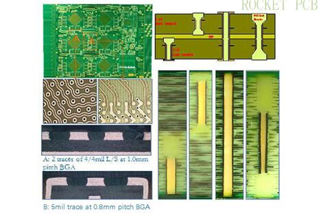
BGA
A ball grid array (BGA) is a surface mount package with a grid of solder balls on the bottom for connection to the PCB.
QFP
A quad flat package (QFP) is a surface mount package with leads extending from all four sides.
| Component Type | Mounting Method |
|---|---|
| Through-Hole | Inserted into holes |
| Surface Mount | Mounted on surface |
| BGA | Grid of solder balls |
| QFP | Leads on four sides |

PCB Manufacturing Terminology
Etching
Etching is the process of removing unwanted copper from the PCB substrate to create the desired traces and pads.
Plating
Plating is the process of depositing a thin layer of metal, usually copper, on the PCB to improve conductivity and protect against corrosion.
Solder Mask
A solder mask is a thin layer of polymer applied to the PCB to protect against oxidation and prevent solder bridges.
Silkscreen
Silkscreen is the process of printing text and symbols on the PCB for identification and assembly purposes.
| Process | Purpose |
|---|---|
| Etching | Remove unwanted copper |
| Plating | Improve conductivity and protection |
| Solder Mask | Prevent oxidation and solder bridges |
| Silkscreen | Print text and symbols |
PCB Design Terminology
Schematic
A schematic is a diagram that represents the electrical connections and components in a circuit.
Footprint
A footprint is the pattern of pads and holes on a PCB that corresponds to a specific component package.
Netlist
A netlist is a text file that describes the connections between components in a PCB design.
Gerber Files
Gerber files are a set of files that contain the necessary information for manufacturing a PCB, including copper layers, solder mask, and silkscreen.
| Term | Definition |
|---|---|
| Schematic | Diagram of electrical connections |
| Footprint | Pattern for a specific component |
| Netlist | Text file of component connections |
| Gerber Files | Manufacturing files |
PCB Testing Terminology
Continuity Test
A continuity test verifies that there are no broken or shorted connections on the PCB.
Functional Test
A functional test verifies that the assembled PCB performs as intended in the final application.
ICT
In-circuit testing (ICT) is a method of testing individual components on an assembled PCB.
AOI
Automated optical inspection (AOI) is a process that uses cameras to visually inspect PCBs for defects.
| Test Type | Purpose |
|---|---|
| Continuity | Check for broken or shorted connections |
| Functional | Verify performance in final application |
| ICT | Test individual components |
| AOI | Visually inspect for defects |
FAQ
1. What is the difference between a single-layer and multi-layer PCB?
A single-layer PCB has copper traces on only one side of the substrate, while a multi-layer PCB has three or more layers of copper traces separated by insulating layers. Multi-layer PCBs offer more complex routing and higher component density compared to single-layer PCBs.
2. What is the purpose of a solder mask on a PCB?
A solder mask is a thin layer of polymer applied to the PCB to protect against oxidation and prevent solder bridges. It covers the copper traces, leaving only the pads and vias exposed for soldering. The solder mask also provides electrical insulation and improves the PCB’s appearance.
3. What are Gerber files, and why are they important?
Gerber files are a set of files that contain the necessary information for manufacturing a PCB. They include data for each copper layer, solder mask, and silkscreen. Gerber files are essential because they provide a standardized format for communicating PCB design information to manufacturers, ensuring accurate and consistent production.
4. What is the difference between through-hole and surface mount components?
Through-hole components have leads that are inserted into holes drilled in the PCB and soldered on the opposite side. Surface mount components, on the other hand, are mounted directly onto the surface of the PCB and soldered to pads. Surface mount components are generally smaller and allow for higher component density compared to through-hole components.
5. What is the purpose of PCB testing, and what are some common testing methods?
PCB testing is essential to ensure that the manufactured board functions as intended and meets the required specifications. Common testing methods include continuity testing to check for broken or shorted connections, functional testing to verify performance in the final application, in-circuit testing (ICT) to test individual components, and automated optical inspection (AOI) to visually inspect for defects. These tests help identify and prevent issues before the PCB is integrated into the final product.
By understanding these common PCB terms and definitions, you can effectively communicate with designers, manufacturers, and customers, ensuring a smooth and successful PCB production process. As PCB technology continues to evolve, staying informed about the latest terminology and industry practices will help you stay ahead in the ever-changing world of electronics.
Leave a Reply