Introduction to PCB Basics
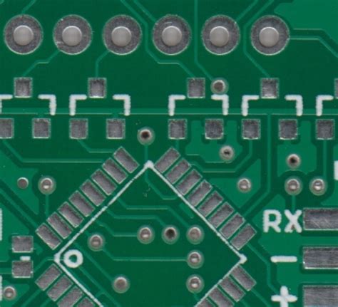
Printed Circuit Boards (PCBs) are the backbone of modern electronic devices. They are used in almost every electronic product, from simple gadgets to complex industrial equipment. PCBs provide a platform for electronic components to be mounted and interconnected, allowing for the creation of complex circuits in a compact and efficient manner. In this article, we will explore the basics of PCB design, including the different types of PCBs, the design process, and best practices for creating reliable and cost-effective PCBs.
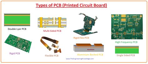
Types of PCBs
There are several types of PCBs, each with its own unique characteristics and applications. The most common types of PCBs include:
Single-layer PCBs
Single-layer PCBs are the simplest and most cost-effective type of PCB. They consist of a single layer of conductive material, usually copper, laminated onto an insulating substrate. Single-layer PCBs are typically used for simple, low-density circuits and are ideal for prototyping and low-volume production.
Double-layer PCBs
Double-layer PCBs have two layers of conductive material, one on each side of the insulating substrate. The two layers are interconnected through plated-through holes (vias). Double-layer PCBs offer higher component density and more complex routing capabilities compared to single-layer PCBs. They are commonly used in a wide range of electronic devices, from consumer electronics to industrial control systems.
Multi-layer PCBs
Multi-layer PCBs consist of three or more layers of conductive material, separated by insulating layers. The layers are interconnected through vias, allowing for even higher component density and more complex routing than double-layer PCBs. Multi-layer PCBs are used in applications that require high performance, such as high-speed digital circuits, RF and microwave devices, and aerospace and defense systems.
Flexible PCBs
Flexible PCBs (FPCBs) are made from flexible insulating materials, such as polyimide or polyester, with conductive traces printed on them. FPCBs can be bent, twisted, and folded to fit into tight spaces or conform to irregular shapes. They are commonly used in applications that require flexibility, such as wearable devices, medical equipment, and automotive electronics.
Rigid-Flex PCBs
Rigid-Flex PCBs combine the benefits of both rigid and flexible PCBs. They consist of rigid PCB sections connected by flexible PCB sections, allowing for three-dimensional packaging and improved reliability. Rigid-Flex PCBs are used in applications that require high density, reliability, and flexibility, such as aerospace, military, and medical devices.
PCB Design Process
The PCB design process involves several key steps, from concept to manufacturing. These steps include:
Schematic Design
The first step in PCB design is to create a schematic diagram of the circuit. The schematic captures the logical connections between components and provides a blueprint for the PCB layout. Schematic design is typically done using Electronic Design Automation (EDA) software, such as Altium Designer, OrCAD, or KiCad.
Component Selection
Once the schematic is complete, the next step is to select the components that will be used in the circuit. Component selection involves choosing parts that meet the electrical, mechanical, and environmental requirements of the design. Factors to consider when selecting components include voltage and current ratings, package size and shape, temperature range, and cost.
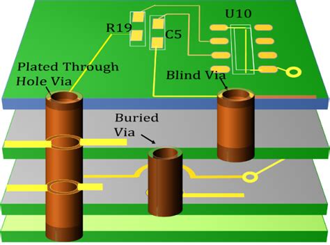
PCB Layout
With the schematic and components in place, the next step is to create the PCB layout. The layout determines the physical placement of components and the routing of traces between them. PCB layout is a critical step in the design process, as it directly affects the performance, reliability, and manufacturability of the final product. Key considerations in PCB layout include:
- Component placement: Components should be placed in a logical and efficient manner, with attention to signal integrity, thermal management, and mechanical constraints.
- Trace routing: Traces should be routed to minimize signal integrity issues, such as crosstalk and electromagnetic interference (EMI), while also meeting manufacturability requirements, such as minimum trace width and spacing.
- Power and ground planes: Power and ground planes should be designed to provide low-impedance paths for power and return currents, while also minimizing EMI and improving signal integrity.
- Vias and through-holes: Vias and through-holes should be used judiciously to minimize signal integrity issues and improve manufacturability.
Design Rule Checking (DRC)
Once the PCB layout is complete, it is important to perform Design Rule Checking (DRC) to ensure that the design meets all manufacturing and reliability requirements. DRC checks the design against a set of predefined rules, such as minimum trace width and spacing, hole size and placement, and copper-to-edge clearance. Any violations of these rules are flagged for correction before the design is sent for manufacturing.
Gerber File Generation
After the design has passed DRC, the final step is to generate Gerber files for manufacturing. Gerber files are industry-standard files that contain all the information needed to fabricate the PCB, including layer images, drill files, and aperture lists. Gerber files are typically generated by the EDA software and sent to the PCB manufacturer for production.

Best Practices for PCB Design
To ensure reliable and cost-effective PCBs, it is important to follow best practices throughout the design process. Some key best practices include:
Keep it simple
Whenever possible, keep the PCB design as simple as possible. Avoid unnecessary complexity, such as excessive layering or dense component placement, which can increase manufacturing costs and reduce reliability.
Use standard components
Using standard components, such as resistors, capacitors, and integrated circuits, can reduce costs and improve availability. Custom or proprietary components should be used only when necessary.
Follow manufacturer guidelines
PCB manufacturers have specific guidelines for designing PCBs that are compatible with their fabrication processes. These guidelines cover topics such as minimum trace width and spacing, hole size and placement, and material selection. Following these guidelines can improve manufacturability and reduce the risk of defects.
Plan for testing
Designing PCBs with testing in mind can greatly simplify the testing process and reduce the risk of defects. This includes adding test points, providing access to critical signals, and designing for automated testing equipment (ATE).
Consider the environment
The environment in which the PCB will be used can have a significant impact on its performance and reliability. Factors to consider include temperature, humidity, vibration, and electromagnetic interference (EMI). Designing PCBs with these factors in mind can improve reliability and reduce the risk of failure in the field.
PCB Design Tools
There are many tools available for designing PCBs, ranging from simple schematic capture tools to full-featured PCB design suites. Some popular PCB design tools include:
| Tool | Description |
|---|---|
| Altium Designer | A full-featured PCB design suite with schematic capture, PCB layout, and 3D modeling capabilities. |
| OrCAD | A widely used PCB design tool with schematic capture, simulation, and PCB layout capabilities. |
| KiCad | A free and open-source PCB design tool with schematic capture, PCB layout, and 3D modeling capabilities. |
| Eagle | A popular PCB design tool with schematic capture, PCB layout, and autorouting capabilities. |
| Fusion 360 | A cloud-based PCB design tool with schematic capture, PCB layout, and mechanical design capabilities. |
FAQ
What is the difference between a PCB and a breadboard?
A breadboard is a prototyping tool used for temporarily building and testing electronic circuits. It consists of a grid of holes that components can be inserted into, with connections made by metal strips underneath. A PCB, on the other hand, is a permanent version of the circuit, with components soldered onto a custom-designed board.
How much does it cost to have a PCB manufactured?
The cost of having a PCB manufactured depends on several factors, including the size and complexity of the board, the number of layers, the quantity ordered, and the turnaround time. In general, small, simple PCBs can cost as little as a few dollars each, while large, complex boards can cost hundreds or even thousands of dollars.
What is the typical turnaround time for PCB manufacturing?
The typical turnaround time for PCB manufacturing depends on the complexity of the board and the manufacturer’s workload. For simple, low-quantity orders, turnaround times can be as short as a few days. For more complex, high-quantity orders, turnaround times can be several weeks or even months.
Can I manufacture my own PCBs at home?
Yes, it is possible to manufacture simple PCBs at home using a process called toner transfer. This involves printing the PCB design onto a special transfer paper using a laser printer, then transferring the toner onto a copper-clad board using heat and pressure. The board is then etched in a chemical solution to remove the unwanted copper, leaving only the desired traces. However, this process is not suitable for complex or high-density designs.
What are some common mistakes to avoid when designing PCBs?
Some common mistakes to avoid when designing PCBs include:
- Forgetting to include test points or access to critical signals
- Using components that are too small or too close together, making assembly and rework difficult
- Failing to consider the environmental factors that can affect the PCB’s performance and reliability
- Not following the manufacturer’s design guidelines, leading to manufacturability issues
- Overcomplicating the design, leading to higher costs and reduced reliability
Conclusion
PCB design is a critical step in the development of electronic products. By understanding the basics of PCB design, including the different types of PCBs, the design process, and best practices, designers can create reliable and cost-effective PCBs that meet the needs of their applications. Whether designing simple, single-layer boards or complex, multi-layer systems, the key to success is a systematic approach that considers all aspects of the design, from schematic capture to manufacturing and testing.
Leave a Reply