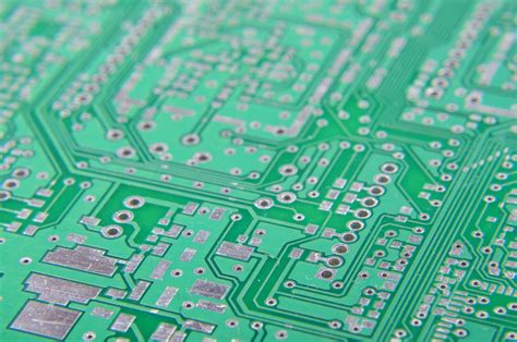
What is a PCB via?
A PCB (Printed Circuit Board) via is a small hole drilled through a PCB that allows electrical connections to be made between different layers of the board. Vias are an essential component of modern PCBs, enabling complex, multi-layered designs in a compact form factor.
PCB vias come in several types, each with its own characteristics and manufacturing process:
| Via Type | Description |
|---|---|
| Through Hole | Drilled through the entire board, connecting all layers |
| Blind | Connects an outer layer to an inner layer, but does not go through the entire board |
| Buried | Connects inner layers, but does not reach the outer layers |
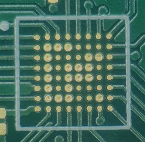
| Micro | A small via, typically less than 0.15mm in diameter, used for high-density designs |
The PCB Via Manufacturing Process
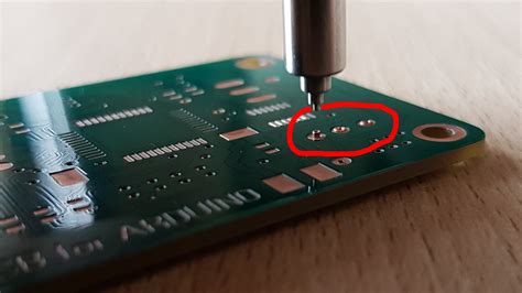
Step 1: Drilling
The first step in creating a PCB via is to drill a hole through the board. This is typically done using a CNC (Computer Numerical Control) drilling machine, which can accurately drill holes as small as 0.1mm in diameter.
The drilling process involves the following sub-steps:
-
Drill file generation: A drill file, containing the location and size of each via, is generated from the PCB design software.
-
Drill bit selection: The appropriate drill bit size is selected based on the via diameter specified in the design.
-
Drilling: The CNC machine drills the holes according to the drill file, ensuring precise location and size.
Step 2: Desmearing
After drilling, the via holes need to be cleaned and prepared for the next step. This process, known as desmearing, removes any debris or resin smear that may be present in the holes.
Desmearing can be done through several methods:
| Method | Description |
|---|---|
| Plasma | Uses a plasma gas to etch away the resin smear |
| Permanganate | A chemical process that dissolves the resin smear |
| Mechanical | Uses abrasive particles to physically remove the resin smear |
Step 3: Electroless Copper Deposition
Once the via holes are cleaned, a thin layer of copper is deposited onto the walls of the holes. This process, known as electroless copper deposition, creates a conductive surface that allows electrical current to flow through the via.
The electroless copper deposition process involves the following steps:
-
Catalyst application: A catalyst solution is applied to the via holes, which helps initiate the copper deposition process.
-
Copper deposition: The PCB is immersed in an electroless copper plating solution, which deposits a thin layer of copper onto the walls of the via holes.
-
Rinsing: The board is rinsed to remove any excess plating solution.
Step 4: Electroplating
After the electroless copper deposition, the via holes are further plated with copper to increase the thickness of the conductive layer. This process, known as electroplating, uses an electric current to deposit additional copper onto the via walls.
The electroplating process involves the following steps:
-
Anode placement: A copper anode is placed in the electroplating solution.
-
Cathode connection: The PCB is connected as the cathode in the electroplating circuit.
-
Current application: An electric current is applied, causing copper ions to migrate from the anode to the cathode (PCB), depositing onto the via walls.
-
Thickness monitoring: The plating thickness is monitored to ensure it meets the specified requirements.
Step 5: Filling (Optional)
In some cases, particularly for high-density designs or to improve thermal dissipation, the via holes may be filled with a conductive material after electroplating. This process, known as via filling, involves the following steps:
-
Via plugging: A conductive paste, typically containing copper or a conductive polymer, is used to fill the via holes.
-
Curing: The filled vias are then cured, typically using heat, to solidify the conductive material.
-
Planarization: The filled vias are planarized, typically through sanding or grinding, to ensure a smooth, even surface.
Types of PCB Vias
Through Hole Vias
Through hole vias are the most common type of via, connecting all layers of the PCB. They are created by drilling a hole through the entire board and plating the walls with copper.
| Advantage | Disadvantage |
|---|---|
| Strong mechanical connection | Consumes more board space |
| Easier to manufacture | Limits routing options on inner layers |
Blind Vias
Blind vias connect an outer layer to one or more inner layers, but do not go through the entire board. They are created by drilling a hole from the surface of the board to a specific inner layer and plating the walls with copper.
| Advantage | Disadvantage |
|---|---|
| Saves board space | More complex to manufacture |
| Allows for higher density designs | Higher cost compared to through hole vias |
Buried Vias
Buried vias connect inner layers of the PCB, but do not reach the outer layers. They are created by drilling a hole between the desired inner layers and plating the walls with copper.
| Advantage | Disadvantage |
|---|---|
| Saves board space | More complex to manufacture |
| Allows for higher density designs | Higher cost compared to through hole vias |
| Improves signal integrity | Requires careful planning during design |
Micro Vias
Micro vias are small vias, typically less than 0.15mm in diameter, used for high-density designs. They can be either blind or buried vias and are often created using laser drilling rather than mechanical drilling.
| Advantage | Disadvantage |
|---|---|
| Enables very high-density designs | Requires specialized manufacturing equipment |
| Improves signal integrity | Higher cost compared to larger vias |
| Reduces EMI (Electromagnetic Interference) | More susceptible to manufacturing defects |

Frequently Asked Questions (FAQ)
1. What is the purpose of a via in a PCB?
A via in a PCB serves as an electrical connection between different layers of the board. It allows signals and power to be routed from one layer to another, enabling more complex and compact PCB designs.
2. What are the different types of PCB vias?
The main types of PCB vias are:
- Through hole vias: Connect all layers of the PCB
- Blind vias: Connect an outer layer to one or more inner layers
- Buried vias: Connect inner layers, but do not reach the outer layers
- Micro vias: Small vias, typically less than 0.15mm in diameter, used for high-density designs
3. How are PCB vias manufactured?
PCB vias are manufactured through a multi-step process that includes:
- Drilling holes in the PCB
- Cleaning and preparing the holes (desmearing)
- Depositing a thin layer of copper onto the hole walls (electroless copper deposition)
- Electroplating the vias to increase the copper thickness
- Optionally filling the vias with a conductive material
4. What are the advantages of using blind or buried vias?
Blind and buried vias offer several advantages over through hole vias:
- They save board space, allowing for higher density designs
- They improve signal integrity by reducing the via stub effect
- They allow for more flexible routing options on inner layers
However, blind and buried vias are more complex to manufacture and have a higher cost compared to through hole vias.
5. What is via filling, and why is it used?
Via filling is the process of filling the via holes with a conductive material, typically copper or a conductive polymer, after electroplating. Via filling is used to:
- Improve thermal dissipation, especially for high-power components
- Enhance structural integrity of the PCB
- Reduce the risk of solder wicking during assembly
- Enable the use of via-in-pad design, where components are placed directly over filled vias
Via filling adds an additional step to the manufacturing process and increases the overall cost of the PCB.
Conclusion
PCB vias are an essential component of modern PCB design, allowing for complex, multi-layered boards in a compact form factor. The manufacturing process for PCB vias involves several steps, including drilling, desmearing, electroless copper deposition, and electroplating. Optional steps, such as via filling, may be used to improve thermal dissipation or enable specific design features.
Different types of vias, such as through hole, blind, buried, and micro vias, offer unique advantages and disadvantages in terms of board space, signal integrity, and manufacturing complexity. Understanding the characteristics and manufacturing process of each via type is essential for designing and producing high-quality, reliable PCBs.
As PCB technology continues to advance, the importance of vias in enabling high-density, high-performance designs will only continue to grow. By staying up-to-date with the latest via manufacturing techniques and design strategies, PCB designers and manufacturers can create innovative, cutting-edge products that meet the demands of an ever-evolving electronics industry.
Leave a Reply