What is a PCB?
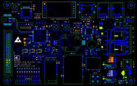
A PCB is a flat board made of insulating material, such as fiberglass or plastic, with conductive pathways printed on its surface. These pathways, also known as traces, connect various electronic components, such as resistors, capacitors, and integrated circuits (ICs), to form a functional circuit.
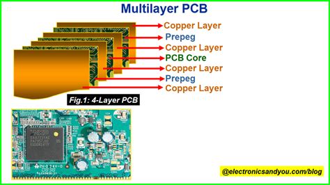
PCBs come in various sizes and shapes, depending on the application. They can be single-sided, with conductive traces on one side only, or double-sided, with traces on both sides. Multi-layer PCBs have several layers of conductive traces separated by insulating material, allowing for more complex circuits in a smaller space.
The PCB Creation Process
The PCB creation process involves several steps, each of which requires specialized knowledge and equipment. Let’s take a closer look at each step.
Step 1: PCB Design
The first step in PCB creation is the design phase. This involves creating a schematic diagram of the circuit, which shows how the various components are connected. The schematic is then used to create a layout of the PCB, which shows the physical placement of the components and the routing of the traces.
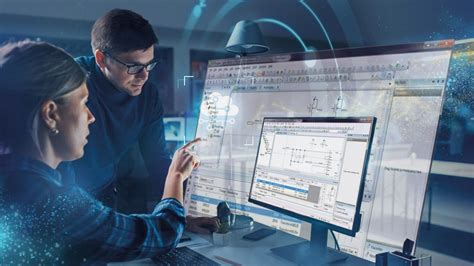
PCB design is typically done using specialized software, such as Altium Designer or KiCad. These tools allow designers to create complex circuits and layouts, and to simulate the behavior of the circuit before it is manufactured.
Step 2: PCB Fabrication
Once the PCB design is complete, the next step is fabrication. This involves creating the physical PCB using a series of chemical and mechanical processes.
The first step in fabrication is to create a copper-clad board, which is a thin layer of copper bonded to an insulating substrate. The copper layer is then coated with a photoresist, which is a light-sensitive material that hardens when exposed to UV light.
The PCB layout is then printed onto a transparency film, which is placed on top of the photoresist-coated board. The board is then exposed to UV light, which hardens the photoresist in the areas where the traces will be. The unhardened photoresist is then washed away, leaving the copper exposed in the desired pattern.
The exposed copper is then etched away using a chemical solution, leaving only the traces behind. The remaining photoresist is then removed, leaving a bare PCB with the desired circuit pattern.
If the PCB is double-sided or multi-layer, additional layers of insulating material and copper are added, and the process is repeated for each layer.
Step 3: PCB Assembly
Once the bare PCB is fabricated, the next step is to assemble the components onto the board. This is typically done using one of two methods: through-hole assembly or surface-mount assembly.
Through-hole assembly involves inserting the leads of the components through holes drilled in the PCB and soldering them in place on the opposite side. This method is typically used for larger components, such as connectors and transformers.
Surface-mount assembly involves placing the components directly onto the surface of the PCB and soldering them in place. This method is typically used for smaller components, such as resistors and capacitors, and allows for higher component density and smaller board sizes.
The components are typically placed onto the PCB using a pick-and-place machine, which uses a vacuum nozzle to pick up the components and place them in the correct position on the board. The board is then passed through a reflow oven, which melts the solder and bonds the components to the board.
Step 4: PCB Testing and Inspection
After the PCB is assembled, it must be tested and inspected to ensure that it functions correctly and meets the required specifications. This involves a series of electrical and visual tests, such as:
- Continuity testing: This involves testing each trace to ensure that it is connected to the correct component and that there are no breaks or shorts in the circuit.
- Functional testing: This involves applying power to the board and testing each function of the circuit to ensure that it operates correctly.
- Visual inspection: This involves inspecting the board for any visible defects, such as solder bridges, missing components, or damaged traces.
If any defects are found, the board is either reworked or scrapped, depending on the severity of the defect and the cost of rework.

PCB Materials and Components
PCBs are made from a variety of materials, each with its own properties and applications. The most common PCB materials are:
- FR-4: This is a glass-reinforced epoxy laminate that is the most widely used PCB material. It has good electrical and mechanical properties, and is suitable for most applications.
- Polyimide: This is a high-performance plastic that is used for high-temperature and high-frequency applications, such as in aerospace and military electronics.
- Teflon: This is a fluoropolymer that is used for high-frequency and microwave applications, due to its low dielectric constant and low loss tangent.
PCBs also use a variety of components, depending on the application. Some common PCB components include:
| Component | Description |
|---|---|
| Resistor | A passive component that resists the flow of electric current. Used to control voltage and current in a circuit. |
| Capacitor | A passive component that stores electric charge. Used to filter and smooth signals, and to store energy. |
| Inductor | A passive component that stores energy in a magnetic field. Used to filter and smooth signals, and to store energy. |
| Diode | A semiconductor component that allows current to flow in only one direction. Used for rectification and protection. |
| Transistor | A semiconductor component that amplifies or switches electronic signals. Used for amplification, switching, and logic. |
| Integrated Circuit (IC) | A miniaturized electronic circuit that performs a specific function. Used for complex functions such as microprocessors and memory. |

PCB Applications
PCBs are used in a wide range of applications, from consumer electronics to industrial automation. Some common PCB applications include:
- Consumer electronics: PCBs are used in smartphones, laptops, televisions, and other consumer devices to connect and control the various components.
- Automotive electronics: PCBs are used in automotive systems such as engine control, infotainment, and safety systems.
- Medical devices: PCBs are used in medical devices such as pacemakers, defibrillators, and imaging equipment.
- Industrial automation: PCBs are used in industrial control systems, such as programmable logic controllers (PLCs) and human-machine interfaces (HMIs).
- Aerospace and defense: PCBs are used in aerospace and defense applications, such as avionics, radar, and communication systems.

Frequently Asked Questions
What is the difference between a PCB and a breadboard?
A breadboard is a temporary prototyping tool used to build and test electronic circuits. It consists of a plastic board with holes that allow components to be inserted and connected without soldering. A PCB, on the other hand, is a permanent circuit board that is used in the final product. It is fabricated using a series of chemical and mechanical processes, and the components are soldered onto the board.
Can I design my own PCB?
Yes, anyone can design their own PCB using specialized software such as Altium Designer or KiCad. However, PCB design requires knowledge of electronics and PCB layout principles, as well as familiarity with the software tools. It is recommended to start with simple designs and work your way up to more complex circuits.
How much does it cost to manufacture a PCB?
The cost of manufacturing a PCB depends on several factors, such as the size of the board, the number of layers, the quantity ordered, and the turnaround time. In general, smaller quantities and faster turnaround times will be more expensive. A simple two-layer board in small quantities (less than 100) can cost anywhere from $50 to $500, while larger quantities and more complex boards can cost thousands of dollars.
What is the difference between through-hole and surface-mount assembly?
Through-hole assembly involves inserting the leads of the components through holes drilled in the PCB and soldering them in place on the opposite side. Surface-mount assembly involves placing the components directly onto the surface of the PCB and soldering them in place. Surface-mount assembly allows for higher component density and smaller board sizes, but requires more precise placement and soldering equipment.
How long does it take to manufacture a PCB?
The time it takes to manufacture a PCB depends on several factors, such as the complexity of the design, the number of layers, and the quantity ordered. In general, simple two-layer boards can be manufactured in as little as 24 hours, while more complex multi-layer boards can take several weeks. Most PCB manufacturers offer standard lead times of 5-15 business days, with expedited options available for an additional cost.
Conclusion
PCB creation is a complex process that requires specialized knowledge and equipment. From design to manufacturing, each step must be carefully planned and executed to ensure a functional and reliable final product.
As electronics continue to become smaller, faster, and more complex, the demand for high-quality PCBs will only continue to grow. By understanding the PCB creation process and the materials and components used, designers and engineers can create innovative and reliable electronic devices that meet the needs of today’s fast-paced world.

Leave a Reply