Introduction to PCB
PCB stands for Printed Circuit Board. It is a fundamental component in modern electronic devices that serves as a platform for connecting and supporting various electronic components. PCBs are found in almost every electronic device we use today, from smartphones and computers to televisions and appliances.
What is a Printed Circuit Board?
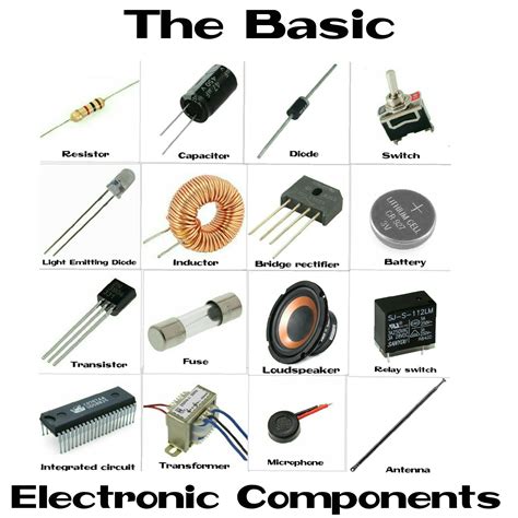
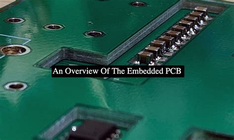
A Printed Circuit Board is a flat, thin board made of insulating materials such as fiberglass, composite epoxy, or other laminate materials. It has conductive pathways, called traces, etched or printed onto its surface to connect different electronic components. These components, such as resistors, capacitors, integrated circuits, and connectors, are soldered onto the board to create a functional electronic circuit.
The Role of PCBs in Electronics
PCBs play a crucial role in the functionality and performance of electronic devices. They provide several key advantages:
-
Compact Design: PCBs allow for the miniaturization of electronic devices by efficiently organizing and connecting components in a compact space.
-
Reliability: The use of PCBs improves the reliability of electronic circuits by providing stable connections and reducing the risk of loose or faulty wiring.
-
Mass Production: PCBs enable the mass production of electronic devices by streamlining the assembly process and reducing manufacturing costs.
-
Signal Integrity: Well-designed PCBs ensure proper signal integrity by minimizing electromagnetic interference and cross-talk between components.
Types of PCBs
There are several types of PCBs, each with its own characteristics and applications. The most common types include:
Single-Layer PCBs
Single-layer PCBs, also known as single-sided PCBs, have conductive traces on only one side of the board. They are the simplest and most cost-effective type of PCB, suitable for basic electronic circuits with low complexity.
Double-Layer PCBs
Double-layer PCBs, or double-sided PCBs, have conductive traces on both sides of the board. They offer more design flexibility and higher component density compared to single-layer PCBs. Double-layer PCBs are commonly used in a wide range of electronic devices, from consumer electronics to industrial applications.
Multi-Layer PCBs
Multi-layer PCBs consist of three or more conductive layers separated by insulating layers. They are used in complex electronic systems that require high component density and advanced signal routing capabilities. Multi-layer PCBs are commonly found in sophisticated devices such as smartphones, computers, and aerospace systems.
Flexible PCBs
Flexible PCBs, or flex PCBs, are made of flexible materials such as polyimide or PEEK. They can bend and twist without damaging the circuit, making them ideal for applications that require flexibility or where space is limited. Flex PCBs are commonly used in wearable devices, medical equipment, and automotive electronics.
Rigid-Flex PCBs
Rigid-flex PCBs combine the benefits of both rigid and flexible PCBs. They consist of rigid sections connected by flexible sections, allowing for three-dimensional packaging and improved reliability in complex electronic assemblies. Rigid-flex PCBs are often used in aerospace, military, and medical applications.
PCB Manufacturing Process
The manufacturing process of PCBs involves several steps to create a functional board. The main stages include:
-
Design: The PCB design is created using specialized software, such as EDA (Electronic Design Automation) tools. The design includes the placement of components, routing of traces, and definition of board layers.
-
Fabrication: The fabrication process begins with the creation of a copper-clad laminate board. The desired circuit pattern is transferred onto the board through a series of chemical etching and plating processes.
-
Drilling: Holes are drilled into the board to accommodate through-hole components and provide interconnections between layers.
-
Solder Mask Application: A solder mask, typically green in color, is applied to the board to protect the copper traces from oxidation and prevent solder bridges during the assembly process.
-
Silkscreen Printing: A silkscreen layer is printed onto the board to add labels, logos, and component identifiers for easier assembly and troubleshooting.
-
Surface Finish: A surface finish, such as HASL (Hot Air Solder Leveling), ENIG (Electroless Nickel Immersion Gold), or OSP (Organic Solderability Preservative), is applied to the exposed copper areas to improve solderability and protect against corrosion.
-
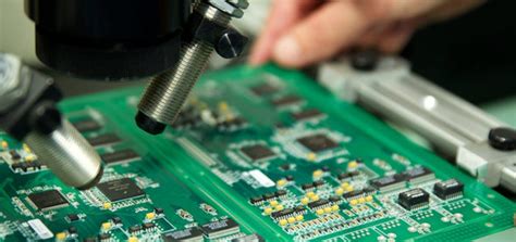
Assembly: The electronic components are mounted onto the PCB through various assembly techniques, such as through-hole mounting or surface mount technology (SMT).
-
Testing: The assembled PCB undergoes rigorous testing to ensure proper functionality, reliability, and compliance with industry standards.

PCB Design Considerations
Designing a PCB requires careful consideration of various factors to ensure optimal performance and reliability. Some key design considerations include:
Component Placement
Proper component placement is crucial for minimizing signal interference, reducing noise, and optimizing thermal management. Components should be placed in a logical and efficient manner, taking into account signal flow, power distribution, and mechanical constraints.
Trace Routing
Trace routing involves creating the conductive pathways that connect components on the PCB. Factors such as trace width, spacing, and impedance control must be considered to maintain signal integrity and minimize crosstalk.
Power and Ground Planes
Dedicated power and ground planes are often incorporated into multi-layer PCBs to provide stable and low-impedance power distribution. These planes help reduce noise, improve signal integrity, and provide shielding between layers.
Thermal Management
Proper thermal management is essential to ensure the reliable operation of electronic components. Techniques such as the use of thermal vias, heatsinks, and careful component placement can help dissipate heat effectively.
Electromagnetic Compatibility (EMC)
EMC considerations are important to minimize electromagnetic interference (EMI) and ensure compliance with regulatory standards. Techniques such as proper grounding, shielding, and the use of filters can help mitigate EMI issues.
PCB Testing and Inspection
Once a PCB is manufactured and assembled, it undergoes various testing and inspection processes to ensure its quality and functionality. Common testing methods include:
Visual Inspection
Visual inspection is the first step in PCB testing. It involves examining the board for any visible defects, such as solder bridges, missing components, or damaged traces. Automated optical inspection (AOI) systems are often used for high-volume production.
Electrical Testing
Electrical testing verifies the electrical continuity and functionality of the PCB. It includes tests such as continuity testing, insulation resistance testing, and functional testing to ensure that the board operates as intended.
In-Circuit Testing (ICT)
ICT is a testing method that involves probing the PCB at various test points to verify the presence, orientation, and value of individual components. It helps detect component-level faults and ensures the correct assembly of the board.
Boundary Scan Testing
Boundary scan testing, also known as JTAG testing, is a method used for testing complex digital circuits. It involves using a test access port (TAP) to control and monitor the inputs and outputs of individual components, enabling the detection of faults and programming of devices.
Burn-In Testing
Burn-in testing involves subjecting the PCB to elevated temperatures and voltages for an extended period to identify early failures and ensure long-term reliability. It helps eliminate infant mortality and improve the overall quality of the product.
PCB Assembly Techniques
PCB assembly involves mounting electronic components onto the board. There are two primary assembly techniques:
Through-Hole Mounting
Through-hole mounting involves inserting the leads of components through holes drilled in the PCB and soldering them to the pads on the opposite side. This technique is suitable for larger components and provides strong mechanical connections.
Surface Mount Technology (SMT)
SMT is a more modern and widely used assembly technique where components are mounted directly onto the surface of the PCB. SMT components have smaller footprints and allow for higher component density compared to through-hole mounting. SMT assembly is typically automated using pick-and-place machines and reflow soldering processes.
Applications of PCBs
PCBs find applications in a wide range of industries and products. Some common applications include:
Consumer Electronics
PCBs are extensively used in consumer electronics such as smartphones, tablets, laptops, televisions, and home appliances. They enable the miniaturization and functionality of these devices.
Automotive Electronics
Modern vehicles rely heavily on electronic systems for various functions such as engine control, infotainment, safety features, and navigation. PCBs are used in automotive electronic control units (ECUs), sensors, and displays.
Industrial Automation
PCBs play a crucial role in industrial automation systems, including programmable logic controllers (PLCs), human-machine interfaces (HMIs), and industrial robots. They enable the control, monitoring, and communication of industrial processes.
Medical Devices
Medical devices such as patient monitors, diagnostic equipment, and implantable devices rely on PCBs for their functionality and reliability. PCBs used in medical applications must meet strict regulatory requirements and standards.
Aerospace and Defense
PCBs used in aerospace and defense applications must withstand harsh environments and meet stringent reliability requirements. They are used in avionics systems, communication equipment, and military vehicles.
Frequently Asked Questions (FAQ)
-
What is the difference between a PCB and a breadboard?
A PCB is a permanent and professionally manufactured board with etched copper traces that connect electronic components. In contrast, a breadboard is a prototyping tool that allows for temporary and reusable connections between components using plug-in wires. -
Can PCBs be repaired if damaged?
Yes, PCBs can be repaired, but the extent of the repair depends on the type and severity of the damage. Minor issues such as broken traces or damaged components can often be repaired using techniques like soldering, wire jumpers, or component replacement. However, extensive damage may require professional repair services or complete board replacement. -
What is the typical turnaround time for PCB manufacturing?
The turnaround time for PCB manufacturing varies depending on factors such as the complexity of the design, the chosen fabrication house, and the manufacturing options selected. Standard lead times range from a few days to several weeks. Expedited services are often available for faster turnaround times, but they come at a higher cost. -
How do I choose the right PCB manufacturer?
When choosing a PCB manufacturer, consider factors such as their experience, capabilities, quality control processes, and customer support. Look for manufacturers with certifications such as ISO 9001 and IPC standards. Request quotes from multiple manufacturers and compare their pricing, lead times, and manufacturing options. Reading reviews and seeking recommendations from experienced designers can also help in making an informed decision. -
What is the minimum feature size achievable in PCB manufacturing?
The minimum feature size in PCB manufacturing refers to the smallest trace width and spacing that can be reliably produced. It depends on the capabilities of the fabrication process and the chosen PCB manufacturer. Typical minimum feature sizes range from 3 to 6 mils (thousandths of an inch) for standard PCB fabrication. Advanced manufacturing processes, such as high-density interconnect (HDI) or micro-via technology, can achieve even smaller feature sizes, down to a few microns.
Conclusion
PCBs are the backbone of modern electronics, enabling the interconnection and functionality of various electronic components. They offer numerous advantages, including compact design, reliability, and mass production capabilities. Understanding the types of PCBs, their manufacturing process, design considerations, and testing methods is crucial for anyone involved in electronic product development.
As technology continues to evolve, PCBs will play an increasingly important role in shaping the future of electronics. From consumer devices to industrial applications, PCBs will continue to enable innovation, miniaturization, and enhanced functionality in the ever-expanding world of electronics.
| PCB Type | Layers | Applications |
|---|---|---|
| Single-Layer PCB | 1 | Simple electronic circuits |
| Double-Layer PCB | 2 | Consumer electronics, industrial applications |
| Multi-Layer PCB | 3+ | Complex devices (smartphones, computers) |
| Flexible PCB | Varies | Wearable devices, medical equipment |
| Rigid-Flex PCB | Varies | Aerospace, military, medical applications |
By understanding the fundamentals of PCBs, designers, engineers, and enthusiasts can leverage their potential to create innovative and reliable electronic products that shape our modern world.
Leave a Reply