Key Functions of a PCB
PCBs serve several critical functions in electronic devices:
- Mechanical support for electronic components
- Electrical connections between components
- Insulation between electrical conductors
- Heat dissipation
- Providing a physical structure and format
1. Providing Mechanical Support
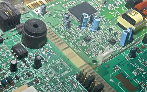
One of the primary purposes of a PCB is to provide a stable platform to securely mount electronic components. Components like integrated circuits, capacitors, resistors, and connectors are soldered directly onto the PCB. The PCB holds everything in place, allowing the circuit to function reliably even when subjected to vibration, impact, or environmental stresses.
2. Enabling Electrical Connections
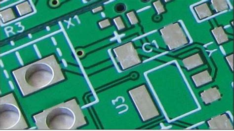
PCBs include conductive pathways known as traces which are etched or printed onto the board to create electrical connections between components. These traces allow electricity and signals to travel from one part of the circuit to another. The conductive copper traces link the leads or pins of the various components soldered to the board. Careful PCB design ensures proper routing of traces to prevent short circuits and minimize electromagnetic interference.
3. Providing Insulation
A PCB substrate is typically made from a non-conductive material like FR4 glass epoxy. This insulating layer prevents unwanted electrical contact between different traces and components. Soldermask applied over the copper traces on the PCB further insulates the conductors. Proper insulation is critical for circuit reliability and safety.
4. Dissipating Heat
As electronic components operate, they generate heat. Excessive heat can lead to component failure or degraded performance. A PCB helps dissipate this heat through copper planes or dedicated heatsinks. Thicker copper layers or additional thermal vias conduct heat away from hot components and spread it across a larger surface area where it can be safely radiated into the environment. Keeping components cool improves circuit stability and longevity.
5. Defining Physical Structure
The size and shape of the PCB itself often defines the overall format of the electronic device. PCBs can be designed to fit within an enclosure of a particular size or to match the form factor of a product. Different types of PCBs cater to various applications:
| PCB Type | Layers | Application |
|---|---|---|
| Single-sided | One copper layer | Simple circuits |
| Double-sided | Two copper layers | Intermediate circuits |
| Multi-layer | Three or more copper layers | Complex/dense circuits |
| Flexible | Flexible substrate | Wearables, tight spaces |
| Rigid-flex | Rigid and flexible sections | Mixed requirements |
The choice of PCB type depends on the complexity of the circuit, space constraints, flexibility needs, and cost considerations.
PCB Design Flow
Creating a PCB involves several steps:
-
Schematic capture: The circuit diagram is drawn using Electronic Design Automation (EDA) software. Component symbols are placed and connected.
-
Board layout: Components are arranged on the board and traces are routed between them. Layers, trace widths, and via placement are defined.
-
DFM check: A Design for Manufacturability review ensures the board can be reliably fabricated.
-
Fabrication: Gerber files are sent to a PCB manufacturer. The blank PCB is fabricated.
-
Assembly: Components are soldered onto the bare board, either through wave soldering, reflow soldering, or by hand.
-
Testing: The assembled board is powered on and functionally tested. Automated Optical Inspection (AOI) may check for manufacturing defects.
Following this process results in a completed PCB assembly ready for integration into an electronic product.
PCB materials
Substrate Materials
The most common base material for rigid PCBs is FR-4 glass epoxy. This is a composite made of woven fiberglass cloth with an epoxy resin binder. FR-4 offers good insulation properties, mechanical strength, and temperature resistance.
Flexible PCBs use substrates like polyimide or PET. These materials can bend and flex without damaging the copper traces. High frequency PCBs may use PTFE/Teflon or Rogers laminates that have lower dielectric loss.
Copper Foil
Copper foil is laminated onto the substrate to create the conductive layer for traces and planes. The thickness of the copper cladding is specified in ounces per square foot. Common thicknesses are:
- 1/2 oz (17.5 microns)
- 1 oz (35 microns)
- 2 oz (70 microns)
Thicker copper allows higher current carrying capacity but is more difficult to etch fine traces.
Soldermask
Soldermask is a polymer coating applied over the copper traces on the PCB. It acts as an insulating layer and prevents solder bridges from forming between closely spaced traces. Soldermask gives PCBs their characteristic green color, although other colors are available. Pads and areas that need to be soldered are left exposed.
Silkscreen
Silkscreen is the white lettering and symbols printed onto the PCB. It is used to label components, show pin 1 indications, display warning symbols, or add logos and branding. Silkscreen ink is applied on top of the soldermask.

PCB Layout Considerations
Designing a PCB layout requires careful planning to ensure proper functionality, manufacturability, and reliability. Some key considerations include:
Trace Routing
Traces should be routed as directly as possible while avoiding sharp angles. The width of the trace depends on the amount of current it needs to carry. High speed signals may require controlled impedance traces. Differential pairs should be length-matched and closely coupled. Trace spacing depends on the voltage difference between them.
Power and Ground Planes
Dedicating full copper layers for power and ground helps reduce electromagnetic interference and provides low impedance current paths. Ground planes also serve as a reference for controlled impedance traces.
Component Placement
Components should be placed in a logical flow that minimizes trace lengths. Decoupling capacitors should be placed close to ICs. Connectors are typically placed along board edges. Thermal considerations may dictate the placement of hot components.
Manufacturing Tolerances
The PCB design must account for the tolerances of the fabrication process. Minimum trace widths, spacing, and drill sizes are determined by the PCB manufacturer’s capabilities. Vias should be sized and spaced appropriately.
Testing and Debugging
Test points and probe pads should be included to allow easy access for debugging. Boundary scan or JTAG test points enable automated testing. Providing a way to probe critical signals can greatly aid in troubleshooting.
FAQ
1. What is the difference between a PCB and a breadboard?
A breadboard is a temporary prototyping tool used to quickly assemble and test electronic circuits. Components are plugged into the holes in the breadboard, and jumper wires make the electrical connections. PCBs are permanent, custom-designed boards that have copper traces connecting the components. PCBs are more reliable, compact, and suitable for finished products.
2. Can PCBs be repaired?
Yes, PCBs can often be repaired, depending on the extent of the damage. Common repairs include resoldering broken connections, replacing damaged components, and adding jumper wires to bypass broken traces. However, complex multi-layer boards can be challenging to repair. Prevention through good design and handling practices is preferred.
3. What are vias in a PCB?
Vias are plated holes that allow traces on different layers of a PCB to connect. A via consists of a barrel with copper plating that extends through the board. Vias can be through-hole (extending all the way through the board) or blind/buried (connecting only certain layers). Vias take up space on the board and can impact signal integrity, so they must be used judiciously.
4. How are surface mount components attached to a PCB?
Surface mount components are attached to a PCB using a soldering process. A solder paste (a mixture of tiny solder balls and flux) is applied to the pads on the PCB. The components are then placed onto the pads, and the board is heated in a reflow oven. The heat melts the solder, permanently attaching the components to the pads. Precise placement and temperature control are essential for reliable solder joints.
5. What is the purpose of solder mask on a PCB?
The Main purpose of solder mask is to insulate the copper traces on the PCB, preventing accidental short circuits. Solder mask is a polymer coating that covers the copper, except in areas where components will be soldered. It also protects the traces from oxidation and damage. Additionally, solder mask helps contain the molten solder during assembly, preventing solder bridges from forming between closely spaced pads or traces.
Conclusion
PCBs are essential to modern electronics, providing a reliable and compact way to assemble circuits. They serve multiple purposes, including mechanical support, electrical connection, insulation, heat dissipation, and defining the physical structure of a device. Understanding the materials, design considerations, and manufacturing processes involved in PCBs is crucial for anyone working in the electronics industry. As electronic devices continue to advance, PCBs will remain at the heart of these innovations, enabling the development of ever more complex and capable systems.
Leave a Reply