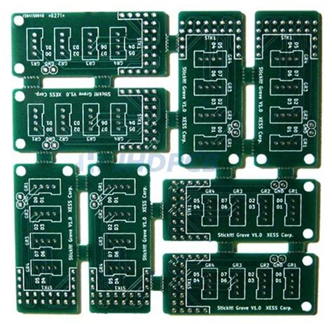
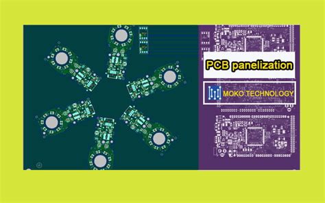
How PCB Panelization Works
The panelization process involves the following key steps:
-
PCB Design: The individual PCB designs are first created using PCB design software. Each PCB design is called a “unit” or “array”.
-
Panelization Layout: Multiple copies of the PCB units are laid out in a grid pattern on a larger “panel”. The panel size is chosen to maximize the number of units that will fit while meeting the manufacturing capabilities. Typically panels are 18×24 inches in size.
-
Tooling: Tooling holes and fiducials are added to the panel. Tooling holes are used to secure the panel during manufacturing and assembly. Fiducials are copper pads used for aligning the panel.
-
Breakaway Tabs: Support tabs, known as breakaway tabs or mouse bites, are added between the individual PCBs. These keep the units secure in the panel during manufacturing. The tabs are cut to separate the individual PCBs after assembly.
-
Copper Pattern: The copper pattern for the panelized design, consisting of the multiple PCB units, is output for manufacturing.
-
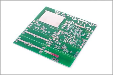
Manufacturing: The panels go through the standard PCB fabrication process of etching, drilling, plating, solder mask application, and silkscreen.
-
Assembly: Components are assembled onto the panel as if it were one large PCB. The individual PCBs are still connected by the breakaway tabs at this stage.
-
Depaneling: After assembly, the individual PCBs are singulated (separated) from the panel by cutting the breakaway tabs. This is often done by breaking the tabs by hand or using a depaneling machine. The individual PCBs are then cleaned and packed for shipping.
Panelization Techniques
There are several different techniques that can be used for panelizing PCB designs:
Tab Routing
Tab routing involves connecting the individual PCBs with small tabs that can be easily cut or broken after manufacturing. The tabs are made by milling slots in a rectangular pattern around each PCB unit. This leaves the small tabs to hold the units in place.
Advantages of tab routing include:
– Secure method of holding units in panel
– Allows individual PCBs to be separated by hand
– Least expensive panelization method
Disadvantages of tab routing include:
– Not suitable for thick PCBs over 1.6 mm
– Tab stubs remain on PCB edges after singulation
– High mechanical stress can damage parts near tabs during breaking
V-Scoring
V-scoring uses a V-shaped cutting wheel to cut 30-35% through the PCB material from both sides, creating a groove where the panel can be easily snapped apart after assembly. The V-grooves are cut along straight lines between the PCB units.
Advantages of V-scoring include:
– Creates a clean, straight edge after breaking
– Suitable for thicker PCBs up to 3.2mm
– Lower mechanical stress on parts compared to tab routing
Disadvantages of V-scoring include:
– Higher cost than tab routing
– Cannot be used on flexible or aluminum-backed PCBs
– Sensitive parts near V-grooves can still be damaged during depaneling
Perforated Lines
Perforated lines, also known as breakaway perforations, are a series of drilled holes that go completely through the panel between the individual PCB units. The holes weaken the panel so it can be easily snapped along the perforations after assembly.
Advantages of perforated lines include:
– Works well for rigid, flexible, and aluminum-backed PCBs
– Clean edges with little material loss
– Minimal stress on parts during depaneling
Disadvantages of perforated lines include:
– Higher cost than routing or V-scoring
– Panels can bow or break prematurely if perforations are too close
– Not suitable for very thin PCBs under 0.8mm
Panelization Methods Comparison
This table summarizes the key characteristics of the 3 main PCB panelization methods:
| Method | Tab Routing | V-Scoring | Perforated |
|---|---|---|---|
| PCB Thickness | ≤ 1.6 mm | ≤ 3.2 mm | 0.8-3.2 mm |
| Edge Quality | Rough with nubs | Straight, clean | Straight, very clean |
| Depaneling Stress | High | Moderate | Low |
| Relative Cost | $ | $$ | $$$ |
Panelization Design Considerations
Several factors must be considered when designing a PCB panel:
Panelization Border
A minimum border of 10-15 mm should be left around the edge of the panel. This provides space for the tooling holes, fiducials, and text markings. It also provides handling room to avoid damaging the individual PCBs.
Tooling Holes
Tooling holes are drilled holes used to register and secure the panel during manufacturing. A minimum of three tooling holes are required, with one hole near the center and the others near opposite corners. The holes are typically 1.5-3.0 mm in diameter.
Fiducials
Fiducials are round copper pads used as alignment markers. There are typically at least three global fiducials on the panel, with one near the center and others near diagonally opposite corners. The fiducials are used to align the panel during solder paste printing and pick-and-place assembly. Local fiducials are also placed on individual PCB units for finer registration.
Breakaway Tabs
For tab-routed designs, slots are milled around each PCB unit leaving breakaway tabs to hold the PCBs in place. The tab width should be 0.7-1.0 mm for easy breaking. Wider tabs may be needed for heavier or thicker PCBs to prevent premature breaking during handling. The spacing between the PCB units, known as the routing gutter, should be 2-3 mm to allow sufficient room for the routing tool.
Text Markings
All PCB panels should be clearly marked with the part number, revision code, and manufacturing date code for traceability. The panel should also have the manufacturer’s logo and contact information. Additional markings like barcodes or QR codes can be added for automatic identification and tracking. All markings should be kept at least 3 mm away from the PCB units.
Minimum Spacing
The minimum spacing between adjacent PCB units depends on the panelization method:
| Panelization Method | Minimum Unit Spacing |
|---|---|
| Tab Routing | 2 mm |
| V-Scoring | 1 mm |
| Perforated | 3 mm |
These spacing guidelines allow room for the breakaway tabs, V-grooves, or perforations between the units while minimizing the waste material.

Assembly Considerations
Panelization introduces some additional considerations during the PCB assembly process:
Solder Paste Printing
A single stencil that covers the entire panel is used for solder paste printing. The stencil openings must align with the pads on all the PCB units across the panel. It is crucial that the PCB units are precisely located within the panel and that there is no warping or bowing of the panel.
Component Placement
A pick-and-place machine is used to automatically place components on the PCB units across the panel. The machine must be programmed with the locations of all the components on each unit and must be able to accurately place the components across the entire panel area. The panel must be consistently located using the fiducials.
Reflow Soldering
During reflow soldering, the entire panel is heated to melt the solder paste and permanently attach the components. The panel must remain flat and rigid during the heating process. Any warping or flexing can cause components to shift out of place. For large panels with many heavy components, a pallet support system may be needed to keep the panel flat during reflow.
Depaneling
After assembly, the individual PCBs have to be depaneled (singulated) from the panel. This is often done manually by breaking or cutting the tabs. Automated depaneling machines are also available which use shearing or milling to separate the PCBs. V-scored and perforated panels are generally easier to depanel than tab-routed panels. Laser cutting can also be used.
Advantages of PCB Panelization
PCB panelization offers several key benefits for volume PCB manufacturing:
-
Reduced Cost: Panelizing multiple PCBs on a single panel reduces the number of individual pieces that need to be handled, saving time and labor costs. Panelization also optimizes material usage, reducing waste.
-
Faster Throughput: Fabricating and assembling one large panel with multiple PCBs is faster than processing many individual PCBs separately. This improves production rates and shortens lead times.
-
Consistent Quality: Producing multiple PCBs on a single panel ensures consistent quality across all the PCBs. The boards experience the same manufacturing conditions and processes.
-
Easier Handling: A panelized array of PCBs is easier to handle than many loose individual boards. This is especially true for very small PCBs, which would be difficult to process on their own.
-
Simplified Assembly: Components can be placed on all the PCBs in a panel in a single automated assembly step. This is much faster and simpler than populating individual PCBs one at a time.
Disadvantages of PCB Panelization
There are also a few potential drawbacks to panelization to be aware of:
-
Design Effort: Panelization adds some extra steps and complexity to the PCB design process. The panel layout must be carefully designed to consider tooling, breakaway tabs, and other manufacturing needs.
-
Minimum Quantities: To be cost-effective, panelization is usually only done for higher production volumes. For prototypes or small quantities, it is often cheaper to produce individual PCBs.
-
Material Waste: While panelization makes efficient use of material, there is still some waste in the borders, tooling areas, and gaps between PCBs. Very small PCBs may have a low ratio of PCB area to waste area on a panel.
-
Depaneling Quality: If not done carefully, the depaneling process can put stress on components near the board edges or leave rough tabs on the PCB edges. Proper panelization design and depaneling methods are needed to ensure quality.
FAQ
What is the typical size of a PCB panel?
Most PCB manufacturers support panel sizes up to 18″ x 24″ (457 x 610 mm). Some can fabricate even larger panels. The actual maximum panel size depends on the manufacturer’s equipment capabilities. Smaller panels like 9″ x 12″ (229 x 305 mm) are also commonly used for less complex boards.
How many PCBs can fit on a panel?
The number of PCBs per panel depends on the size of the individual PCB and the panelization method. A rough estimate can be made by dividing the panel area by the area of one PCB plus the required spacing. For example, a 100 x 100 mm PCB panelized with 3 mm spacing would fit about 20 PCBs on a 9″ x 12″ panel:
(9″ x 12″) / ((100 mm + 3 mm) x (100 mm + 3 mm)) ≈ 20 PCBs
Can different PCB designs be panelized together?
Yes, different PCBs can be mixed on the same manufacturing panel as long as they use the same materials and layer stackup. This allows the PCBs to go through the fabrication process together. However, the assembly steps would have to be done separately for each unique design on the panel. Mixed panels are sometimes used for prototype runs to save cost.
Are there any PCBs that cannot be panelized?
Most standard rigid PCBs can be panelized. Flexible circuits can also be panelized using specialized methods. However, very thick PCBs over 3.2 mm or boards with large heavy components may be difficult or impossible to panelize. Boards with tight tolerances or complex mechanical requirements may also be better fabricated individually. The PCB manufacturer can advise on the panelization feasibility for a specific design.
How much does panelization add to the cost?
The cost of panelization depends on the complexity of the panel and the number of PCBs per panel. Simple tab-routed panels may only add a few cents per PCB for large quantities. More complex panels with custom routing, V-scoring, or perforation can add $ 0.10-0.20 per PCB. However, this added cost is usually more than offset by the savings from fabricating and assembling the PCBs in a panelized format. A cost analysis should be done to compare individual and panelized pricing for a specific project.
Conclusion
PCB panelization is a powerful technique for streamlining PCB manufacturing and assembly. By grouping multiple PCBs onto a single panel, production rates can be significantly increased while reducing costs. Panelization does require some additional design effort and has some limitations, but for most volume applications the benefits outweigh the tradeoffs. Following good panelization design practices and working closely with the PCB fabricator will ensure successful implementation of panelization in PCB production.
Leave a Reply