Introduction to PCB Layers
Printed Circuit Boards (PCBs) are the backbone of modern electronics. They provide a platform for mounting and interconnecting electronic components to create a functional circuit. One of the key decisions in PCB design is choosing the appropriate number of layers. In this article, we will focus on the differences between 2 layer and 4 layer PCBs, and help you determine when to choose one over the other.
What are PCB Layers?
PCB layers refer to the number of conductive copper layers that make up the board. Each layer is separated by an insulating material, typically FR-4, which is a flame-retardant glass-reinforced epoxy laminate. The copper layers are etched with the desired circuit pattern and interconnected through vias, which are small holes drilled through the board and plated with conductive material.
Types of PCB Layers
There are several types of PCB layers, each with its own characteristics and applications:
| Layer Type | Description |
|---|---|
| Signal | Used for routing signals between components |
| Power | Provides a stable power supply to the components |
| Ground | Serves as a reference point for the circuit and helps reduce noise |
| Mixed | Combines signal, power, and ground on a single layer |
2 Layer PCB
A 2 layer PCB consists of two copper layers, one on the top and one on the bottom of the board. The top layer is typically used for component placement and signal routing, while the bottom layer is used for ground and power distribution.
Advantages of 2 Layer PCB
-
Lower Cost: 2 layer PCBs are generally less expensive to manufacture compared to multilayer boards due to their simpler construction and fewer materials required.
-
Easier to Design: With fewer layers to consider, 2 layer PCBs are easier to design and layout. This can lead to faster development times and lower design costs.
-
Suitable for Simple Circuits: 2 layer PCBs are ideal for simple circuits with low component density and minimal interconnections.
Disadvantages of 2 Layer PCB
-
Limited Routing Space: With only two layers available, routing can become challenging as the circuit complexity increases. This can lead to longer signal paths and potential signal integrity issues.
-
Higher Electromagnetic Interference (EMI): The lack of dedicated ground and power planes in 2 layer PCBs can result in higher EMI, which can affect the performance of sensitive components.
-
Lower Current Carrying Capacity: The limited copper area on a 2 layer PCB restricts the amount of current that can be carried, which may not be sufficient for power-hungry applications.
4 Layer PCB
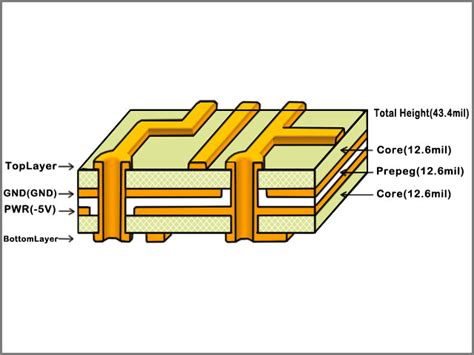
A 4 layer PCB consists of four copper layers, typically arranged as signal, ground, power, and signal layers. This configuration provides better signal integrity, reduced EMI, and increased routing flexibility compared to 2 layer PCBs.
Advantages of 4 Layer PCB
-
Improved Signal Integrity: The dedicated ground and power planes in a 4 layer PCB provide a low-impedance return path for signals, reducing crosstalk and improving signal quality.
-
Reduced EMI: The ground and power planes act as shields, minimizing electromagnetic interference both within the board and with external devices.
-
Higher Current Carrying Capacity: With more copper area available, 4 layer PCBs can handle higher currents, making them suitable for power-intensive applications.
-
Increased Routing Flexibility: The additional layers in a 4 layer PCB provide more routing space, allowing for denser component placement and shorter signal paths.
Disadvantages of 4 Layer PCB
-
Higher Cost: The increased complexity and materials required for 4 layer PCBs result in higher manufacturing costs compared to 2 layer boards.
-
Longer Fabrication Time: The additional layers and processing steps involved in 4 layer PCB production can lead to longer fabrication times.
-
More Complex Design: Designing a 4 layer PCB requires careful consideration of layer stackup, via placement, and signal routing, which can be more challenging than designing a 2 layer board.

Factors to Consider When Choosing Between 2 Layer and 4 Layer PCB
When deciding between a 2 layer and 4 layer PCB, several factors should be taken into account:
-
Circuit Complexity: As the complexity of your circuit increases, with higher component density and more interconnections, a 4 layer PCB becomes more advantageous due to its increased routing flexibility and signal integrity.
-
Frequency and Speed: High-frequency and high-speed signals are more susceptible to noise and interference. A 4 layer PCB’s dedicated ground and power planes help mitigate these issues, making them a better choice for such applications.
-
Power Requirements: If your circuit requires high current or has multiple power supplies, a 4 layer PCB’s increased copper area and dedicated power plane can provide better power distribution and heat dissipation.
-
EMI Considerations: Applications sensitive to electromagnetic interference, such as medical devices or automotive electronics, may benefit from the improved EMI shielding provided by a 4 layer PCB.
-
Size Constraints: In space-constrained designs, the increased routing density of a 4 layer PCB can help minimize board size while accommodating all necessary components and connections.
-
Budget and Time: 2 layer PCBs are generally less expensive and faster to manufacture than 4 layer boards. If your project has strict budget or time constraints, a 2 layer PCB may be the more practical choice, as long as it meets your circuit’s performance requirements.
FAQ
-
Q: Can I use a mix of through-hole and surface-mount components on a 2 layer PCB?
A: Yes, both through-hole and surface-mount components can be used on a 2 layer PCB. However, the limited routing space may make it more challenging to accommodate a high number of through-hole components, which require additional space for drill holes and pads. -
Q: Are 4 layer PCBs always better than 2 layer PCBs?
A: Not necessarily. While 4 layer PCBs offer several advantages, such as improved signal integrity and reduced EMI, they may not be the best choice for every application. Simple circuits with low component density and relaxed performance requirements can often be adequately served by a well-designed 2 layer PCB. -
Q: Can I convert a 2 layer PCB design to a 4 layer PCB?
A: In most cases, yes. However, converting a 2 layer PCB design to a 4 layer PCB will require adjustments to the layer stackup, via placement, and routing. It’s essential to carefully review and optimize the design to ensure proper signal integrity and manufacturability. -
Q: How do I determine the appropriate layer stackup for a 4 layer PCB?
A: The optimal layer stackup for a 4 layer PCB depends on various factors, such as the signal types, frequencies, and power requirements of your circuit. A common stackup is signal-ground-power-signal, which provides good signal integrity and EMI performance. Consulting with your PCB manufacturer or an experienced PCB designer can help determine the best layer stackup for your specific application. -
Q: Are there any special considerations for designing a 4 layer PCB?
A: When designing a 4 layer PCB, it’s essential to pay close attention to via placement and routing to ensure proper signal integrity and manufacturability. This includes minimizing via stubs, avoiding unnecessary layer transitions, and following best practices for high-speed signal routing. Additionally, it’s crucial to work closely with your PCB manufacturer to ensure that your design meets their fabrication capabilities and guidelines.
Conclusion
Choosing between a 2 layer and 4 layer PCB is an important decision that can significantly impact the performance, reliability, and cost of your electronic device. By understanding the advantages and disadvantages of each option and carefully considering your circuit’s requirements, you can make an informed choice that balances functionality, manufacturability, and budget.
In general, 2 layer PCBs are a cost-effective solution for simple circuits with low component density and relaxed performance requirements. They offer lower manufacturing costs and faster turnaround times, making them suitable for prototyping and low-volume production.
On the other hand, 4 layer PCBs provide superior signal integrity, reduced EMI, and increased routing flexibility, making them the preferred choice for more complex circuits, high-speed applications, and power-intensive designs. While they come with higher costs and longer fabrication times, the improved performance and reliability they offer can be well worth the investment.
Ultimately, the decision between a 2 layer and 4 layer PCB should be based on a thorough analysis of your specific circuit requirements, taking into account factors such as complexity, frequency, power, EMI, size, and budget. By carefully weighing these considerations and consulting with experienced PCB designers and manufacturers, you can ensure that your chosen PCB layer configuration will provide the optimal balance of performance, reliability, and cost for your application.
Leave a Reply