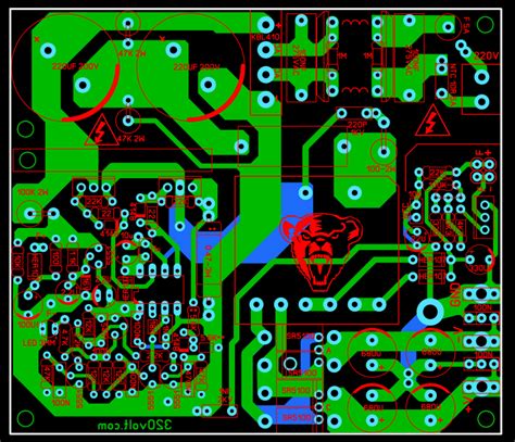
Understanding the Basics of SMPS PCB Layout
Before diving into the specific guidelines, it’s important to understand the basic principles of SMPS PCB layout. An SMPS consists of several key components, including:
- Power transformer
- Switching devices (MOSFETs or IGBTs)
- Rectifier diodes
- Output filter capacitors
- Control circuitry
The primary goal of SMPS PCB layout is to minimize the loop areas of high-frequency currents, reduce parasitic inductances, and provide proper grounding and shielding. By following these principles, you can minimize EMI, reduce noise, and improve the overall performance of your SMPS.
Key Guidelines for SMPS PCB Layout
1. Component Placement
Proper component placement is essential for minimizing loop areas and reducing parasitic inductances. Follow these guidelines for optimal component placement:
- Place the power transformer, switching devices, and rectifier diodes close to each other to minimize the loop area of high-frequency currents.
- Position the output filter capacitors as close to the rectifier diodes as possible to reduce the loop area and minimize ripple voltage.
- Place the control circuitry away from the high-current paths to avoid interference.
2. Grounding and Power Planes
Proper grounding and power plane design are crucial for minimizing EMI and ensuring stable operation. Consider these guidelines:
- Use a solid ground plane to provide a low-impedance return path for high-frequency currents.
- Separate the ground plane into two sections: power ground (PGND) and signal ground (SGND). Connect PGND and SGND at a single point, preferably near the output filter capacitors.
- Use separate power planes for different voltage levels to minimize coupling and interference.
3. Trace Routing and Widths
Trace routing and widths play a significant role in reducing parasitic inductances and minimizing EMI. Follow these guidelines:
- Use wide traces for high-current paths to minimize resistance and inductance.
- Keep the traces for the power stage as short as possible to reduce loop areas.
- Route the sensitive control signals away from the high-current paths to avoid interference.
- Use a star-point connection for the power and ground traces to minimize voltage drops and ensure stable operation.
4. Shielding and Isolation
Shielding and isolation techniques help reduce EMI and prevent interference between different sections of the SMPS. Consider these guidelines:
- Use shielding techniques, such as copper pours or shield cans, to isolate the high-frequency components from the rest of the circuit.
- Provide adequate isolation between the primary and secondary sides of the power transformer to meet safety requirements and prevent noise coupling.
- Use isolated feedback circuitry to prevent noise from the secondary side from affecting the primary side control circuitry.
5. Filtering and Decoupling
Filtering and decoupling techniques help reduce noise and ensure stable operation. Follow these guidelines:
- Use input and output filters to attenuate high-frequency noise and meet EMI regulations.
- Place decoupling capacitors close to the power pins of ICs to provide a low-impedance path for high-frequency currents and minimize noise.
- Use ferrite beads or inductors in series with the power lines to suppress high-frequency noise.
PCB Layer Stackup for SMPS
A well-designed PCB layer stackup is essential for minimizing EMI and ensuring proper signal integrity. Here’s a recommended 4-layer stackup for an SMPS:
| Layer | Purpose |
|---|---|
| Top | Component placement, signal routing |
| Inner 1 | Power plane (e.g., +12V) |
| Inner 2 | Ground plane (PGND and SGND) |
| Bottom | Component placement, signal routing |
This stackup provides a solid ground plane for low-impedance return paths and separate power planes for different voltage levels. The signal layers are placed on the top and bottom layers to allow for easy component placement and routing.

SMPS PCB Layout Checklist
To ensure that you have covered all the essential aspects of SMPS PCB layout, use this checklist:
- Minimize loop areas of high-frequency currents
- Place components strategically to reduce parasitic inductances
- Use solid ground and power planes
- Separate PGND and SGND, connecting them at a single point
- Use wide traces for high-current paths
- Route sensitive control signals away from high-current paths
- Implement shielding and isolation techniques
- Use input and output filters to reduce EMI
- Place decoupling capacitors close to IC power pins
- Use a well-designed PCB layer stackup
By following this checklist and the guidelines discussed in this article, you can create a robust and efficient SMPS PCB layout that minimizes EMI, reduces noise, and ensures optimal performance.
Frequently Asked Questions (FAQ)
1. What is the main purpose of SMPS PCB layout?
The main purpose of SMPS PCB layout is to minimize electromagnetic interference (EMI), reduce noise, and ensure optimal performance by minimizing loop areas, reducing parasitic inductances, and providing proper grounding and shielding.
2. Why is component placement important in SMPS PCB layout?
Component placement is crucial in SMPS PCB layout because it helps minimize loop areas and reduce parasitic inductances. By placing components strategically, such as keeping the power transformer, switching devices, and rectifier diodes close together, you can minimize the loop area of high-frequency currents and improve overall performance.
3. What is the difference between PGND and SGND?
PGND (power ground) is the ground plane section dedicated to the high-current power stage of the SMPS, while SGND (signal ground) is the ground plane section used for sensitive control circuitry. Separating PGND and SGND helps minimize noise coupling between the power stage and control circuitry.
4. How can shielding and isolation techniques help in SMPS PCB layout?
Shielding and isolation techniques help reduce EMI and prevent interference between different sections of the SMPS. Copper pours or shield cans can be used to isolate high-frequency components from the rest of the circuit. Proper isolation between the primary and secondary sides of the power transformer is also essential to meet safety requirements and prevent noise coupling.
5. What is the recommended PCB layer stackup for an SMPS?
A recommended 4-layer stackup for an SMPS includes a top layer for component placement and signal routing, an inner layer for the power plane, another inner layer for the ground plane (PGND and SGND), and a bottom layer for component placement and signal routing. This stackup provides a solid ground plane for low-impedance return paths and separate power planes for different voltage levels, while allowing for easy component placement and routing on the outer layers.
By following the guidelines and best practices outlined in this article, you can create a well-designed SMPS PCB layout that minimizes EMI, reduces noise, and ensures optimal performance for your power supply.
Leave a Reply