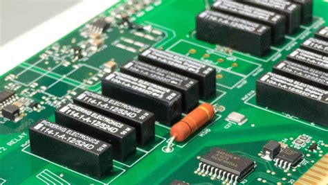
What is PCB Modularization?
PCB modularization is the process of breaking down a complex printed circuit board (PCB) design into smaller, more manageable modules or blocks. Each module represents a specific function or sub-system of the overall design. By adopting a modular approach, PCB designers can simplify the design process, improve reusability, and streamline development and manufacturing.
Benefits of PCB Modularization
Implementing a modular approach to PCB design offers several key benefits:
-
Simplified Design Process: By breaking down the design into smaller modules, designers can focus on one section at a time, making the overall process more manageable and less overwhelming.
-
Increased Reusability: Modular designs allow for the reuse of specific modules across multiple projects, saving time and effort in future designs.
-
Improved Collaboration: With a modular approach, different team members can work on separate modules simultaneously, enhancing collaboration and reducing development time.
-
Easier Debugging and Maintenance: Modularized designs make it easier to identify and resolve issues, as each module can be tested and debugged independently.
-
Faster Time-to-Market: By simplifying the design process and enabling parallel development, PCB modularization can help reduce overall development time and accelerate product launches.
Steps to Implement PCB Modularization
To successfully implement a modular approach in your PCB design process, follow these steps:
Step 1: Identify Functional Blocks
Begin by analyzing your PCB design and identifying the main functional blocks or sub-systems. These blocks should represent distinct functions or features of your product. Examples of functional blocks include power supply, microcontroller, sensor interfaces, communication modules, and user interfaces.
Step 2: Define Module Interfaces
Once you have identified the functional blocks, define the interfaces between the modules. Determine how the modules will communicate and exchange data with each other. Clearly specify the input and output signals, power requirements, and any necessary control signals for each module.
Step 3: Develop Module Specifications
Create detailed specifications for each module, including its functionality, performance requirements, and physical dimensions. Consider factors such as signal integrity, power consumption, and thermal management when defining the module specifications.
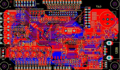
Step 4: Design Individual Modules
With the module specifications in place, start designing each module independently. Focus on optimizing the layout, component placement, and routing within each module. Ensure that the modules adhere to the defined interfaces and specifications.
Step 5: Verify and Test Modules
Once the individual modules are designed, verify and test each module thoroughly. Conduct simulations, prototyping, and physical testing to ensure that the modules function as intended and meet the specified requirements. Identify and resolve any issues or incompatibilities at this stage.
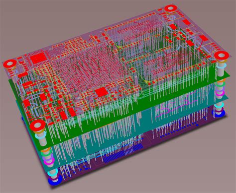
Step 6: Integrate Modules
After verifying the individual modules, integrate them into the complete PCB design. Ensure proper connectivity and compatibility between the modules. Conduct overall system-level simulations and testing to validate the integrated design.
Step 7: Optimize and Iterate
Review the integrated design and identify areas for optimization. Look for opportunities to further simplify the design, reduce component count, or improve signal integrity. Iterate on the design as necessary, making adjustments to the modules and their interfaces based on feedback and testing results.

Best Practices for PCB Modularization
To maximize the benefits of PCB modularization, consider the following best practices:
-
Standardize Interfaces: Develop standardized interfaces between modules to ensure compatibility and reusability across different projects.
-
Use Hierarchical Design: Employ a hierarchical design approach, where each module is treated as a separate entity with its own schematic and layout files.
-
Document Modules: Maintain clear and comprehensive documentation for each module, including its functionality, interfaces, and any specific requirements or constraints.
-
Version Control: Implement version control practices to track changes and revisions to individual modules and the overall design.
-
Collaborate with Manufacturers: Engage with PCB manufacturers early in the design process to ensure that your modularized design is compatible with their manufacturing capabilities and guidelines.
Examples of PCB Modularization
To illustrate the concept of PCB modularization, let’s consider a few examples:
Example 1: Smart Home Hub
A smart home hub is a device that connects and controls various smart home devices, such as lights, thermostats, and security systems. By applying PCB modularization, the design can be broken down into the following modules:
| Module | Description |
|---|---|
| Power Supply | Provides stable and regulated power to all modules |
| Microcontroller | Central processing unit for device control and communication |
| Wi-Fi Module | Enables wireless connectivity to the smart home network |
| Zigbee Module | Facilitates communication with Zigbee-based smart devices |
| Bluetooth Module | Allows connection to Bluetooth-enabled devices |
| Ethernet Module | Provides wired network connectivity |
| User Interface | Includes buttons, LEDs, and display for user interaction |
By designing each module separately and defining clear interfaces, the development of the smart home hub becomes more manageable and efficient.
Example 2: Automotive Infotainment System
An automotive infotainment system combines entertainment, navigation, and communication features in a vehicle. PCB modularization can be applied to simplify the design process:
| Module | Description |
|---|---|
| Power Management | Handles power distribution and regulation for the system |
| Processor Module | Main processing unit for running the infotainment software |
| Display Module | Drives the display for user interface and visual output |
| Audio Module | Manages audio input and output, including amplification |
| GPS Module | Enables navigation and location-based services |
| Connectivity Module | Provides connectivity options (e.g., Bluetooth, Wi-Fi, USB) |
| Tuner Module | Handles radio tuning and reception |
By breaking down the infotainment system into modular components, designers can focus on optimizing each module independently, leading to a more efficient and streamlined development process.
FAQ
Q1: How does PCB modularization differ from traditional PCB design?
A1: PCB modularization involves breaking down the design into smaller, independent modules, each representing a specific function or sub-system. Traditional PCB design often treats the entire board as a single entity, which can be more complex and difficult to manage.
Q2: Can PCB modularization be applied to all types of PCB designs?
A2: PCB modularization can be applied to most types of PCB designs, especially those with complex functionality or multiple sub-systems. However, the extent of modularization may vary depending on the specific requirements and constraints of the project.
Q3: How does PCB modularization impact the cost of PCB design and manufacturing?
A3: While PCB modularization may require additional upfront planning and design effort, it can lead to cost savings in the long run. Modularized designs often result in simplified manufacturing processes, reduced assembly time, and improved yield rates. Additionally, the reusability of modules across projects can further reduce development costs.
Q4: What are the challenges associated with PCB modularization?
A4: Some challenges of PCB modularization include defining clear and compatible interfaces between modules, ensuring proper signal integrity and power management across modules, and managing the increased complexity of documentation and version control. Overcoming these challenges requires careful planning, communication, and adherence to best practices.
Q5: Can PCB modularization be combined with other design methodologies?
A5: Yes, PCB modularization can be combined with other design methodologies, such as design for manufacturing (DFM), design for testability (DFT), and design for reliability (DFR). Incorporating these methodologies alongside modularization can further enhance the efficiency, quality, and reliability of the PCB design process.
By adopting a modular approach to PCB design, you can simplify the design process, improve reusability, and accelerate product development. By following the steps outlined in this article and adhering to best practices, you can successfully implement PCB modularization in your projects and reap the benefits of a more streamlined and efficient design workflow.
Leave a Reply