Introduction to PCB Schematic Design
Designing a printed circuit board (PCB) schematic is a crucial step in the process of creating a functional electronic device. A well-designed PCB schematic serves as a blueprint for the physical layout of the board, ensuring that all components are correctly connected and the circuit operates as intended. Altium Designer is a powerful tool for creating PCB schematics and layouts, offering a wide range of features and capabilities to streamline the design process.
In this article, we will guide you through the steps of creating a PCB schematic using Altium Designer, covering essential concepts, best practices, and tips to optimize your design.
Understanding the Basics of PCB Schematics
What is a PCB Schematic?
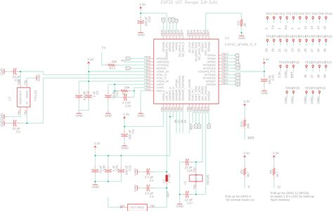
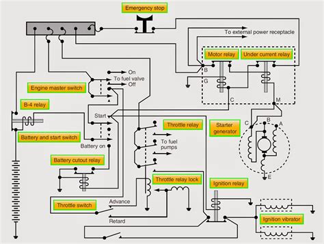
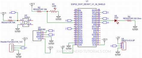
A PCB schematic is a graphical representation of an electronic circuit, displaying the interconnections between various components such as resistors, capacitors, integrated circuits (ICs), and connectors. The schematic serves as a logical diagram of the circuit, focusing on the electrical connections rather than the physical layout of the components.
The Importance of a Well-Designed PCB Schematic
A well-designed PCB schematic is essential for several reasons:
- It provides a clear and concise representation of the circuit, making it easier for designers, engineers, and technicians to understand the circuit’s functionality.
- It enables efficient troubleshooting and debugging by allowing users to trace signals and identify potential issues.
- It serves as a foundation for the physical PCB layout, ensuring that components are correctly placed and connected.
Setting Up Your Altium Designer Project
Creating a New Project
To begin creating your PCB schematic in Altium Designer, you first need to create a new project:
- Open Altium Designer and click on “File” in the top menu.
- Select “New” and then choose “Project.”
- In the “New Project” dialog box, select “PCB Project” and give your project a name.
- Choose a location to save your project and click “OK.”
Configuring Project Settings
Before diving into the schematic design, it’s important to configure your project settings to ensure consistency and adherence to design standards:
- In the “Projects” panel, right-click on your project name and select “Project Options.”
- In the “Project Options” dialog box, navigate through the various categories (such as “Parameters,” “Error Reporting,” and “Comparator”) and adjust the settings according to your project requirements and company guidelines.

Creating Your PCB Schematic
Adding Components to Your Schematic
To begin building your PCB schematic, you’ll need to add components to your design:
- In the “Libraries” panel, locate the library containing the component you wish to add.
- Drag and drop the component from the library onto your schematic sheet.
- Repeat this process for all the components required in your circuit.
Connecting Components with Wires
Once you have added the necessary components, you’ll need to connect them using wires:
- Select the “Wire” tool from the toolbar or press the “W” key on your keyboard.
- Click on the first pin you want to connect and then click on the second pin to create a wire between them.
- Continue connecting pins until all the necessary connections are made.
Adding Labels and Annotations
To improve the readability and clarity of your schematic, add labels and annotations to your components and wires:
- Select the “Label” tool from the toolbar or press the “L” key on your keyboard.
- Click on the component or wire you wish to label and type the desired text.
- Use the “Comment” tool (press “K” on your keyboard) to add additional notes or annotations to your schematic.
Creating Hierarchical Blocks
For complex designs, it’s often beneficial to create hierarchical blocks to simplify your schematic and improve organization:
- Select the components you wish to group into a hierarchical block.
- Right-click on the selection and choose “Create Sheet Symbol.”
- Give the sheet symbol a name and click “OK.”
- The selected components will now be represented by a single hierarchical block, which can be expanded by double-clicking on it.
Verifying and Validating Your PCB Schematic
Running Design Rule Checks (DRC)
To ensure your PCB schematic adheres to design rules and constraints, run a Design Rule Check (DRC):
- In the top menu, click on “Tools” and select “Design Rule Check.”
- In the “Design Rule Check” dialog box, select the rules you wish to check and click “Run DRC.”
- Review any errors or warnings generated by the DRC and make the necessary corrections to your schematic.
Performing Electrical Rule Checks (ERC)
In addition to DRCs, it’s crucial to perform Electrical Rule Checks (ERC) to verify the electrical integrity of your design:
- In the top menu, click on “Tools” and select “Electrical Rule Check.”
- In the “Electrical Rule Check” dialog box, select the rules you wish to check and click “Run ERC.”
- Address any issues identified by the ERC to ensure your schematic is electrically sound.
Best Practices for PCB Schematic Design
Organizing Your Schematic
To maintain a clean and easily navigable schematic, follow these organization tips:
- Use a logical and consistent component placement strategy, such as grouping related components together or arranging them in the order of signal flow.
- Utilize multiple schematic sheets for complex designs, and use hierarchical blocks to simplify the top-level schematic.
- Minimize wire crossovers and keep wires as short and straight as possible to improve readability.
Naming Conventions and Annotation
Adopt a consistent and descriptive naming convention for your components, nets, and labels:
- Use meaningful names that reflect the component’s function or the net’s purpose.
- Follow industry-standard naming conventions, such as using “R” for resistors, “C” for capacitors, and “U” for integrated circuits.
- Annotate your components with unique designators (e.g., R1, R2, C1, U1) to easily identify them in both the schematic and the physical PCB layout.
Documentation and Version Control
Proper documentation and version control are essential for collaborative design and future reference:
- Include a title block on each schematic sheet with relevant information such as the project name, designer name, date, and revision number.
- Use the comment tool to add notes and explanations for complex or non-standard design decisions.
- Utilize a version control system (e.g., Git, SVN) to track changes and collaborate with team members effectively.
Transitioning from Schematic to PCB Layout
Generating a Bill of Materials (BOM)
Before transitioning to the PCB layout, generate a Bill of Materials (BOM) to ensure all necessary components are accounted for:
- In the top menu, click on “Reports” and select “Bill of Materials.”
- Configure the BOM options, such as the output format and the information to include.
- Generate the BOM and review it to ensure all components are listed correctly.
Assigning Footprints to Components
To prepare for the physical PCB layout, assign footprints to each component in your schematic:
- Double-click on a component to open its properties dialog box.
- In the “Footprint” field, select the appropriate footprint for the component from the available libraries.
- Repeat this process for all components in your schematic.
Generating a Netlist
A netlist is a text file that describes the connectivity of your schematic and is used to transfer information to the PCB layout:
- In the top menu, click on “Design” and select “Update PCB Document.”
- Choose the PCB layout document to update and click “OK.”
- The netlist will be generated, and your schematic information will be transferred to the PCB layout.
Frequently Asked Questions (FAQ)
1. What is the difference between a PCB schematic and a PCB layout?
A PCB schematic is a logical representation of an electronic circuit, focusing on the electrical connections between components. In contrast, a PCB layout is the physical representation of the circuit, showing the actual placement and routing of components on the printed circuit board.
2. How do I import a component from a new library into my Altium Designer project?
To import a component from a new library:
1. In the “Libraries” panel, right-click and select “File” > “Add Library.”
2. Navigate to the location of the library file and click “Open.”
3. The library will be added to your project, and its components will be available for use in your schematic.
3. What should I do if I encounter an error during the Design Rule Check (DRC)?
If you encounter an error during the DRC:
1. Double-click on the error message in the “Messages” panel to locate the error in your schematic.
2. Carefully review the error description and the affected components or connections.
3. Make the necessary corrections to your schematic to resolve the error.
4. Re-run the DRC to ensure the error has been successfully resolved.
4. Can I create custom components in Altium Designer?
Yes, you can create custom components in Altium Designer:
1. In the top menu, click on “File” and select “New” > “Library.”
2. Choose “Schematic Library” and click “OK.”
3. Use the available tools to create your custom component symbol and define its properties.
4. Save the library and add it to your project to use the custom component in your schematic.
5. How can I collaborate with team members on a PCB schematic design in Altium Designer?
To collaborate with team members on a PCB schematic design:
1. Use a version control system (e.g., Git, SVN) to share and manage your project files.
2. Establish clear communication channels and design guidelines to ensure consistency and minimize conflicts.
3. Utilize Altium Designer’s built-in collaboration features, such as the “Comment” tool and the “Project History” panel, to share feedback and track changes.
4. Regularly synchronize your local project files with the version control system to stay up-to-date with your team’s progress.
Conclusion
Creating a PCB schematic in Altium Designer is a critical step in the electronic design process, laying the foundation for a successful PCB layout and a functional end product. By following the steps and best practices outlined in this article, you can design efficient, well-organized, and error-free PCB schematics.
Remember to start by setting up your project correctly, carefully placing and connecting components, and utilizing features like hierarchical blocks and annotation to improve readability and organization. Regularly run Design Rule Checks (DRC) and Electrical Rule Checks (ERC) to verify your design’s integrity, and maintain proper documentation and version control for effective collaboration and future reference.
With practice and attention to detail, you’ll be able to create professional-grade PCB schematics in Altium Designer, paving the way for successful PCB layouts and innovative electronic products.
Word count: 1960
Leave a Reply