Introduction to Gerber Files and Altium Designer
Gerber files are the industry standard for PCB fabrication, providing a universal format for defining the layout and design of printed circuit boards. Altium Designer, a powerful PCB design software, allows you to create high-quality schematics and PCB layouts, and generate Gerber files for manufacturing. In this comprehensive guide, we will walk you through the step-by-step process of generating Gerber files in Altium Designer, starting from the schematic design and ending with a production-ready PCB.
Understanding the PCB Design Workflow in Altium Designer
Before diving into the Gerber file generation process, it’s essential to understand the PCB design workflow in Altium Designer. The typical workflow consists of the following steps:
- Schematic design
- PCB layout
- Design rule checks (DRC)
- Gerber file generation
Schematic Design
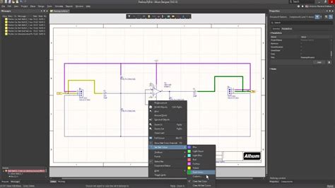
The schematic design is the first step in the PCB design process. It involves creating a graphical representation of the circuit, including components, connections, and hierarchical blocks. Altium Designer provides a user-friendly schematic editor with a vast library of components and symbols, making it easy to create complex designs.
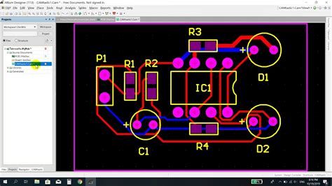
PCB Layout
Once the schematic design is complete, you can proceed to the PCB layout stage. In this step, you’ll arrange the components on the PCB, route the traces, and define the board stackup. Altium Designer offers a range of tools and features to streamline the PCB layout process, such as interactive routing, design rule checks, and 3D visualization.
Design Rule Checks (DRC)
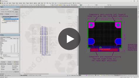
Before generating Gerber files, it’s crucial to perform design rule checks (DRC) to ensure that your PCB layout adheres to the manufacturing constraints and design guidelines. Altium Designer provides a comprehensive set of design rules that you can customize based on your specific requirements. Running DRC helps identify and resolve any potential issues, such as clearance violations, unconnected nets, or insufficient copper coverage.
Gerber File Generation
With a completed and verified PCB layout, you can now generate Gerber files for manufacturing. Gerber files contain all the necessary information for PCB fabrication, including copper layers, solder mask, silkscreen, and drill data. Altium Designer allows you to generate Gerber files in various formats, such as RS-274X or X2, depending on your fabricator’s requirements.
Step-by-Step Guide to Generating Gerber Files in Altium Designer
Now that you have a basic understanding of the PCB design workflow let’s dive into the step-by-step process of generating Gerber files in Altium Designer.
Step 1: Complete the Schematic Design
- Open Altium Designer and create a new project.
- Design your schematic using the schematic editor. Add components, create connections, and define hierarchical blocks as needed.
- Verify the schematic design by running electrical rule checks (ERC) to ensure that there are no connectivity issues or design errors.
Step 2: Create the PCB Layout
- Create a new PCB document within your Altium Designer project.
- Transfer the schematic design to the PCB layout using the “Update PCB Document” command.
- Arrange the components on the PCB, considering factors such as component placement, routing, and manufacturing constraints.
- Route the traces between the components using Altium Designer’s interactive routing tools. Ensure that you adhere to the design rules and guidelines.
- Define the board stackup, including the number of layers, layer thicknesses, and material properties.
Step 3: Perform Design Rule Checks (DRC)
- Open the PCB Rules and Constraints Editor in Altium Designer.
- Define the design rules based on your manufacturing requirements, such as minimum clearances, trace widths, and via sizes.
- Run the design rule checks (DRC) to identify any violations or potential issues in your PCB layout.
- Resolve any DRC errors or warnings by modifying the PCB layout accordingly.
Step 4: Configure the Gerber File Output Settings
- Go to the “File” menu in Altium Designer and select “Fabrication Outputs” > “Gerber Files.”
- In the Gerber Setup dialog box, configure the output settings based on your fabricator’s requirements. This includes:
- Selecting the appropriate Gerber format (e.g., RS-274X or X2)
- Choosing the layers to include in the Gerber output (e.g., copper layers, solder mask, silkscreen)
- Defining the aperture settings and file extensions
- Specifying the output directory for the generated Gerber files
- Click “OK” to save the Gerber file output settings.
Step 5: Generate the Gerber Files
- In the Gerber Setup dialog box, click the “Generate” button to create the Gerber files.
- Altium Designer will generate the Gerber files based on your output settings and save them in the specified output directory.
Step 6: Verify the Generated Gerber Files
- Open the generated Gerber files using a Gerber viewer, such as the built-in Gerber viewer in Altium Designer or a third-party viewer like GC-Prevue or ViewMate.
- Carefully review each layer of the Gerber files to ensure that they accurately represent your PCB layout.
- Check for any missing or incorrect features, such as unintended gaps, overlaps, or incorrect pad sizes.
Step 7: Package and Send the Gerber Files to Your PCB Fabricator
- Compress the generated Gerber files into a ZIP archive.
- Include any additional files or documentation required by your PCB fabricator, such as drill files, assembly drawings, or bill of materials (BOM).
- Send the packaged Gerber files to your chosen PCB fabricator for manufacturing.

Common Issues and Troubleshooting Tips for Gerber File Generation in Altium Designer
While generating Gerber files in Altium Designer is generally a straightforward process, you may encounter some common issues along the way. Here are a few troubleshooting tips to help you overcome these challenges:
Issue 1: Missing or Incorrect Layers in Gerber Output
If you notice that certain layers are missing or incorrect in your generated Gerber files, double-check your Gerber file output settings. Ensure that you have selected the appropriate layers to include in the output and that the layer names and file extensions match your fabricator’s requirements.
Issue 2: Incorrect Aperture Settings
Incorrect aperture settings can lead to issues with pad sizes, trace widths, or clearances in your manufactured PCB. Verify that your aperture settings in the Gerber Setup dialog box are consistent with your design requirements and fabricator’s specifications. If unsure, consult with your fabricator for guidance.
Issue 3: Design Rule Violations
If your PCB layout contains design rule violations, it may result in manufacturing issues or reduced reliability. Always run a comprehensive design rule check (DRC) before generating Gerber files. Resolve any DRC errors or warnings by modifying your PCB layout to adhere to the design rules and guidelines.
Issue 4: Incompatible Gerber Format
Different PCB fabricators may have specific requirements for the Gerber file format. Ensure that you generate Gerber files in the format compatible with your chosen fabricator. Common formats include RS-274X and X2. Consult with your fabricator to determine their preferred format and any additional requirements.
| Gerber Format | Description |
|---|---|
| RS-274X | The most widely used Gerber format, also known as Extended Gerber or Gerber X |
| X2 | An advanced Gerber format that includes embedded aperture definitions and supports complex shapes |
Frequently Asked Questions (FAQ)
1. What are Gerber files, and why are they important for PCB manufacturing?
Gerber files are the standard file format used in the PCB industry to describe the layout and design of a printed circuit board. They contain all the necessary information for PCB fabrication, including copper layers, solder mask, silkscreen, and drill data. Gerber files are essential because they provide a universal format that allows PCB fabricators to manufacture your design accurately and consistently.
2. Can I generate Gerber files directly from the schematic in Altium Designer?
No, you cannot generate Gerber files directly from the schematic in Altium Designer. Gerber files are generated from the PCB layout, which is created based on the schematic design. The schematic represents the logical connections and components, while the PCB layout defines the physical arrangement and routing of those components on the board.
3. What is the difference between RS-274X and X2 Gerber formats?
RS-274X, also known as Extended Gerber or Gerber X, is the most widely used Gerber format. It supports a variety of aperture shapes and sizes and is compatible with most PCB fabricators. On the other hand, X2 is an advanced Gerber format that includes embedded aperture definitions and supports complex shapes. X2 offers improved efficiency and eliminates the need for separate aperture list files. However, not all fabricators may support the X2 format.
4. How do I ensure that my Gerber files are compatible with my PCB fabricator’s requirements?
To ensure compatibility with your PCB fabricator’s requirements, follow these steps:
- Consult with your fabricator and obtain their specific Gerber file requirements, such as preferred format, layer naming conventions, and file extensions.
- Configure the Gerber file output settings in Altium Designer according to your fabricator’s specifications.
- Generate a set of sample Gerber files and send them to your fabricator for review and validation before proceeding with the full manufacturing run.
- Maintain clear communication with your fabricator throughout the process to address any concerns or requirements.
5. Can I include additional information, such as assembly drawings or bill of materials, along with the Gerber files?
Yes, you can include additional information along with the Gerber files when sending them to your PCB fabricator. Many fabricators require or appreciate supplementary files, such as:
- Assembly drawings: Provides a visual reference for component placement and orientation on the PCB.
- Bill of materials (BOM): Lists all the components used in the design, including their quantities, part numbers, and values.
- Drill files: Contains information about the size, location, and type of holes to be drilled in the PCB.
- Readme file: Includes any special instructions, notes, or requirements for the fabricator.
When packaging your Gerber files, include these additional files in the same ZIP archive or provide them as separate files, depending on your fabricator’s preferences.
Conclusion
Generating Gerber files in Altium Designer is a critical step in the PCB design process, as it enables you to transform your schematic and PCB layout into a format that can be manufactured by PCB fabricators. By following the step-by-step guide outlined in this article, you can easily generate high-quality Gerber files that accurately represent your PCB design.
Remember to start with a well-designed schematic, create a proper PCB layout, and perform thorough design rule checks before generating the Gerber files. Pay attention to your fabricator’s requirements and configure the Gerber file output settings accordingly. Verify the generated Gerber files using a Gerber viewer to ensure accuracy and completeness.
By understanding the importance of Gerber files and mastering the generation process in Altium Designer, you can streamline your PCB design workflow, minimize errors, and achieve successful manufacturing results. Happy PCB designing!
Leave a Reply