Introduction to Circuit Board Prototyping
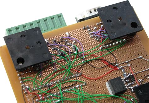
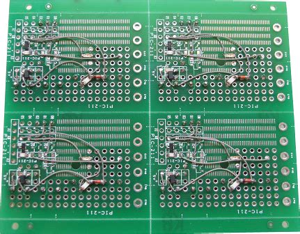
Circuit board prototyping is a critical part of the electronics design process. Before committing to a final printed circuit board (PCB) design for mass production, engineers need to test and validate their designs through prototypes. Traditionally, PCB prototypes have been fabricated using subtractive manufacturing methods like milling or etching. However, these methods can be slow and expensive, especially for complex designs.
In recent years, 3D printing has emerged as a promising alternative for rapid and low-cost PCB prototyping. By leveraging additive manufacturing techniques, 3D printers can fabricate custom circuit boards layer by layer, allowing for faster iteration and more design flexibility compared to traditional methods.
How 3D Printing Works for Circuit Boards
3D printing, also known as additive manufacturing, builds objects by depositing material in successive layers based on a digital 3D model. For PCBs, the 3D printer typically uses conductive and insulating materials to create the desired circuit patterns and substrate.
There are several 3D printing technologies that can be used for PCB Fabrication, including:
-
Fused Deposition Modeling (FDM): FDM printers use a heated nozzle to extrude thermoplastic filaments, which are deposited layer by layer to form the object. For PCBs, conductive filaments like graphene or metal-filled plastics can be used to print the circuit traces, while standard filaments like PLA or ABS can be used for the insulating substrate.
-
Stereolithography (SLA): SLA printers use a laser to cure and harden liquid photopolymer resin layer by layer. For PCBs, conductive resins can be used to print the circuit traces, while standard resins can be used for the insulating substrate.
-
Selective Laser Sintering (SLS): SLS printers use a laser to sinter powdered materials into a solid object. For PCBs, conductive powders like metal or graphene can be used to print the circuit traces, while insulating powders like nylon or ceramics can be used for the substrate.
The choice of 3D printing technology depends on factors like the desired resolution, material properties, and cost. FDM is generally the most affordable and accessible option, while SLA and SLS offer higher resolution and more material options but at a higher cost.
Advantages of 3D Printing for Circuit Prototyping
3D printing offers several key advantages over traditional PCB prototyping methods:
-
Speed: 3D printing can fabricate PCB prototypes in a matter of hours, compared to days or weeks for traditional methods. This allows for faster iteration and testing of designs.
-
Cost: 3D printing is generally more affordable than traditional methods for small-batch prototypes, as there are no setup costs or minimum order quantities. This makes it ideal for startups, hobbyists, and educational institutions.
-
Design Flexibility: 3D printing allows for more complex and customized PCB designs, as it is not limited by the constraints of subtractive manufacturing. This includes non-planar geometries, embedded components, and multi-material structures.
-
In-House Fabrication: With a desktop 3D printer, PCB prototypes can be fabricated in-house, reducing lead times and reliance on external manufacturers. This is especially valuable for sensitive or proprietary designs.
Here is a comparison table of 3D printing vs traditional PCB prototyping methods:
| Factor | 3D Printing | Traditional (Milling/Etching) |
|---|---|---|
| Speed | Hours | Days to Weeks |
| Cost (Low Volume) | $ | $$$ |
| Design Flexibility | High | Low |
| In-House Fabrication | Yes | No |
| Resolution | Medium | High |
| Material Options | Limited | Wide |
As the table shows, 3D printing excels in speed, cost, and design flexibility, while traditional methods still offer advantages in resolution and material options. The choice ultimately depends on the specific requirements and constraints of the project.

Limitations and Challenges of 3D Printed Circuit Boards
Despite its advantages, 3D printing PCBs also has some limitations and challenges that need to be considered:
-
Conductivity: The conductivity of 3D printed traces is generally lower than that of traditional copper traces. This can limit the current carrying capacity and high-frequency performance of the circuit.
-
Resolution: The resolution of 3D printers is generally lower than that of traditional PCB manufacturing methods. This can limit the minimum feature size and spacing of the circuit traces.
-
Material Properties: The material properties of 3D printed PCBs, such as thermal conductivity, dielectric constant, and mechanical strength, may not match those of traditional PCB materials. This can impact the performance and reliability of the circuit.
-
Post-Processing: 3D printed PCBs often require post-processing steps, such as sintering, plating, or polishing, to improve their conductivity and surface finish. This can add time and complexity to the fabrication process.
-
Scalability: While 3D printing is well-suited for prototyping and low-volume production, it may not be economical or practical for high-volume manufacturing due to its slower speed and higher cost per unit compared to traditional methods.
To overcome these limitations, researchers and companies are actively developing new materials, processes, and design strategies for 3D printed PCBs. For example, using hybrid 3D printing methods that combine conductive inks with insulating substrates can improve the conductivity and resolution of the circuits. Optimizing the design for 3D printing, such as using thicker traces and larger pad sizes, can also help mitigate some of the limitations.
Applications and Examples of 3D Printed Circuit Boards
Despite its limitations, 3D printing has already found various applications in PCB prototyping and low-volume production. Some examples include:
-
Rapid Prototyping: 3D printing allows engineers to quickly test and iterate on new PCB designs, reducing the time and cost of product development. This is especially valuable in fields like consumer electronics, aerospace, and medical devices, where fast innovation is critical.
-
Customized and Complex Designs: 3D printing enables the fabrication of PCBs with non-standard geometries, such as curved or flexible surfaces, embedded components, and multi-layer structures. This opens up new possibilities for wearable electronics, IoT devices, and other applications where traditional PCB designs are limited.
-
Education and Research: 3D printing makes PCB fabrication more accessible and affordable for students, hobbyists, and researchers. This democratizes electronics innovation and enables more people to learn about circuit design and manufacturing.
-
Low-Volume Production: For niche products or custom designs that require only a small number of PCBs, 3D printing can be more economical than traditional manufacturing methods. This is especially relevant for industries like aerospace, defense, and medical devices, where low-volume, high-mix production is common.
Here are some specific examples of 3D printed PCBs:
-
Researchers at Duke University used 3D printing to fabricate a flexible, wireless sensor for measuring blood flow in the brain. The 3D printed PCB allowed them to create a customized, conformal design that could be implanted in a rat’s brain.
-
Nano Dimension, an Israeli company, offers a 3D printer specifically designed for multi-layer PCBs. Their DragonFly LDM system can print complex circuits with conductive and insulating materials, enabling rapid prototyping and low-volume production.
-
Voltera, a Canadian startup, developed a desktop 3D printer for fabricating Single-Layer PCBs. Their V-One printer uses conductive ink and an insulating substrate to create custom circuits in minutes, making it ideal for hobbyists and educators.
As 3D printing technology continues to advance, we can expect to see more applications and examples of 3D printed PCBs in various industries and domains.
FAQ
- What materials are used for 3D printing PCBs?
For the conductive traces, common materials include metal-filled filaments (e.g., copper, silver, graphene), conductive resins, and sintered metal powders. For the insulating substrate, standard 3D printing materials like PLA, ABS, nylon, and photopolymers are used.
- How long does it take to 3D print a PCB?
The printing time depends on the size and complexity of the PCB design, as well as the specific 3D printing technology used. For a simple, single-layer PCB, printing can take as little as 30 minutes. For more complex, multi-layer designs, printing can take several hours.
- What is the resolution of 3D printed PCBs?
The resolution depends on the specific 3D printer and material used. For FDM printers, the typical resolution is around 100-400 microns, while SLA and SLS printers can achieve higher resolutions of 25-100 microns. This is generally lower than the resolution of traditional PCB manufacturing methods, which can achieve trace widths and spacings of 50 microns or less.
- Can 3D printed PCBs be used for high-frequency circuits?
The lower conductivity and resolution of 3D printed traces can limit their performance in high-frequency applications. However, by optimizing the design and using advanced materials and processes, 3D printed PCBs have been demonstrated for circuits operating up to several GHz.
- How much does it cost to 3D print a PCB?
The cost depends on the size and complexity of the PCB, as well as the specific 3D printer and materials used. For a simple, single-layer PCB, the material cost can be as low as a few dollars. The cost of the 3D printer itself ranges from a few hundred dollars for desktop FDM printers to tens of thousands of dollars for high-end SLA or SLS printers. However, for low-volume prototypes, the cost per PCB is generally lower than traditional manufacturing methods, which have high setup costs and minimum order quantities.
Conclusion
3D printing is a promising technology for rapid and low-cost PCB prototyping. By leveraging additive manufacturing techniques, 3D printers can fabricate custom circuit boards with more design flexibility and faster turnaround times compared to traditional methods. While there are still limitations in terms of conductivity, resolution, and material properties, ongoing research and development are pushing the boundaries of what is possible with 3D printed PCBs.
As the technology continues to evolve, we can expect to see more applications and examples of 3D printed PCBs in various industries, from consumer electronics to aerospace to medical devices. Whether for rapid prototyping, customized designs, or low-volume production, 3D printing is democratizing electronics innovation and enabling more people to bring their ideas to life.
If you’re interested in exploring 3D printing for your own PCB projects, there are many resources available online, from tutorials and forums to design tools and service providers. With a little experimentation and iteration, you can unlock the full potential of 3D printing for fast and flexible circuit prototyping.
Leave a Reply